(1985) Participation in the first experimental demonstration of the Aharonov-Bohm quantum interference effect
in semiconductor nanostructures as a graduate student in Purdue University.
(1987) Development of a method to couple drift-diffusion models and Monte Carlo
models of device simulation as a graduate student in Purdue University.
(1994) Proposal for Single Spin Logic (SSL), where the spin of a single electron is used to encode
classical binary bit information. Classical logic gates are implemented by engineering the spin-spin interactions
between single electrons confined in semiconductor quantum dots. Progenitor of spin-based quantum computing.
(1994-present) Development of several electrochemical techniques to produce extremely well ordered
regimented arrays of nanostructures. These nanostructures have been employed for electronic, optical and
spintronic devices. This work was featured in the 1997 US Army Nanoscience Poster (prepared for the Pentagon)
as one of four most significant advancements made in nanoscience that year. It has been featured in national
and internal press (newspapers,
magazines, television, radio, and internet blogs) and led to US Patent 5,747,180 granted May 5, 1998.
(1996) Proposal for using a single electron spin in a quantum dot for a qubit and design of a quantum
inverter. This is among
the first proposals for using spins in quantum dots for qubits but does not present a universal
quantum gate.
(1996-present) Proposal, design and study of neuromorphic computing architectures based on interacting
nanowires. This work was initiated in 1996 in collaboration with Purdue, UCLA, Notre Dame and University of
Nebraska, and became a continuing collaboration with researchers at University of Michigan-Ann Arbor.
In 2003, researchers in the Quantum Device Laboratory demonstrated negative differential resistance
(both N-type and S-type) in self assembled arrays of nanowires, which forms the basis of this architecture.
A year later, optically modulated negative differential resistance in these
nanowires was demonstrated stimulating interest in optically programmed networks and sensor-processor fusion.
(1998) Experimental demonstration of giant second-order non-linear dielectric susceptibility in
self-assembled CdS quantum dots. The susceptibility is five times larger than that found in bulk CdS.
Possible applications are in extremely low threshold optical limiters, switches, couplers, mixers, frequency
converters and
optical logic elements. (This work was performed in collaboration with Kurchatov Institute, Moscow, Russia).
(1997-2000) Experimental demonstration of extremely high magnetic coercivity in quantum dots of cobalt,
alpha-iron and iron/cobalt alloys. This has applications in making thermally stable magnetic data storage
disks with a bit density approaching 100 Gbits/in2. (Work performed
in collaboration with Prof. David J. Sellmyer’s group in Dept. of Physics, University of Nebraska-Lincoln).
(2000) Experimental discovery of a novel room-temperature electronic bistability in self-assembled
semiconductor nanowires. The nanowires exhibit two stable, non-volatile conductance states whose conductances
differ by four orders of magnitude. This has applications in extremely high density static random access
memory. The storage times exceed 5 years at room temperature. (Work performed in collaboration with
Kurchatov Institute, Moscow, Russia). Led to US Patent 6,501,676 granted December 31, 2002 which has been
commercially
licensed. This device is a progenitor of the “memristor” which is currently a major area of research.
(2000) Theoretical prediction of the “noise squeezing effect” made possible by phonon engineering in quantum wires.
Noise squeezing can depress the noise floor in microwave devices and circuits by 2-3 orders of magnitude.
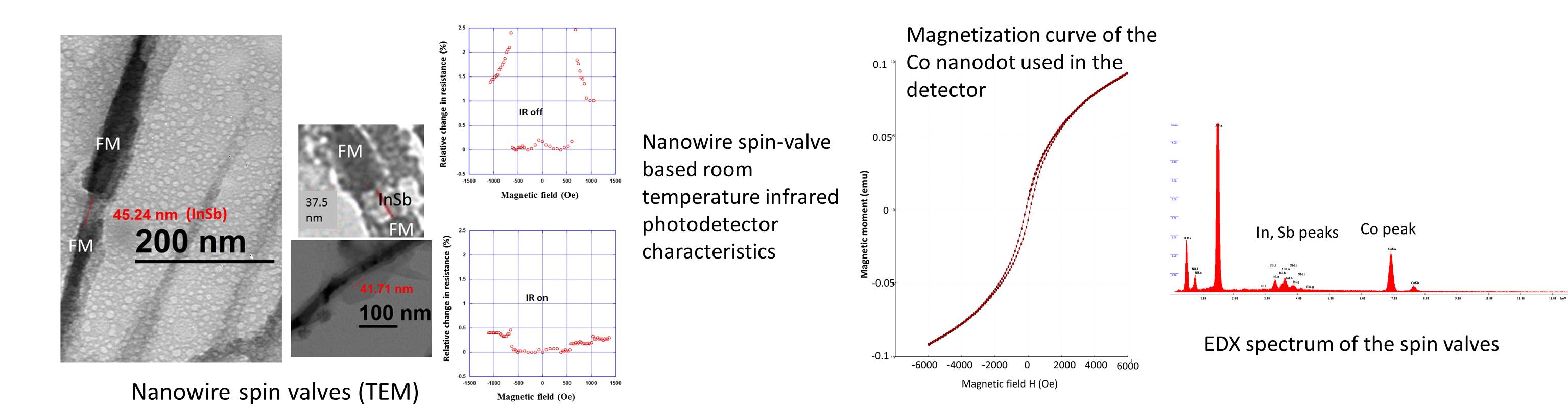
(2000) Experimental demonstration of a novel room temperature infrared photodetector based
on real space transfer in semiconductor quantum wires self-assembled in anodic alumina templates.
This photodetector had an on/off ratio of 160:1 corresponding to a signal-to-noise ratio of 45 dB.
Subsequent work in this area (2011) resulted in the demonstration of the first dual infrared/ultraviolet
nanowire detector (with measured room temperature infrared
detectivity D* exceeding 10^7 Jones). This work has led to US patent 8,946,678 granted February 3, 2015.
(2006) First experimental demonstration of tri-modal self-assembly leading to the simultaneous
self-assembly of nanowires, quantum dots and nanodomes on the same wafer. Later extended to carbon
“nanonecklaces” and gold “nano-pine-trees”. Work was done in collaboration with University of Cincinnati,
National Research Council of Canada, Université Lyon (France) and the Wright Patterson Air Force Laboratory.
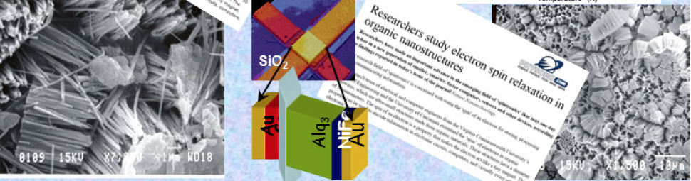
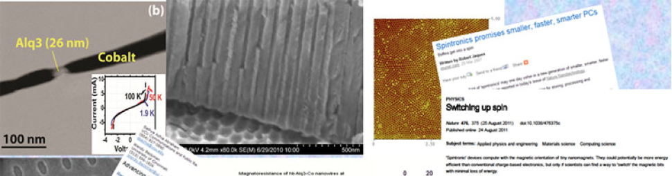
(2007) Experimental demonstration of exceptionally long spin relaxation time of up to 1 second in
organic nanostructures at 100 K. This is the longest spin relaxation time demonstrated in any nanosystem
above liquid
nitrogen temperature. Work done in collaboration with Prof. Marc Cahay’s group in University of Cincinnati.
(2007) Experimental demonstration of the phonon bottleneck effect in organic nanostructures.
(2008) Experimental demonstration of giant increase in the metal enhanced fluorescence in organic and
biological molecules fashioned into nanowires. This work has applications in bio-detection and biosensing. (Work performed in
collaboration with Prof. Gary Tepper in Department of Mechanical
Engineering at VCU and Dr. John Anderson of the US Army Engineer Research and Development Center, Alexandria, VA).
(2010) Discovery of a nearly universal 1/f^2 spectrum of mobility fluctuation noise in semiconductor
quantum wires based on Monte Carlo simulation (theoretical).
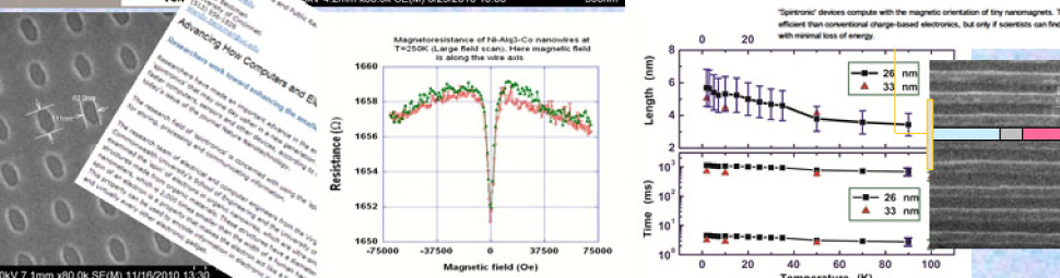
(2010) Development of the field of hybrid spintronics and straintronics where voltage generated
strain is used to rotate the magnetizations of multiferroic nanomagnets (magnetostrictive elastically coupled
to piezoelectric). Work was done in collaboration with Prof. Jayasimha Atulasimha in the Department of
Mechanical and
Nuclear Engineering at Virginia Commonwealth University. Led to US patent 8,921,962 granted December 30, 2014.
(2013) First experimental demonstration of the spin Hanle effect at room temperature in single
subband nanowires.
Significant for the implementation of “spin transistors” based on modulation of spin-orbit interaction.
Work performed with Prof. Jayasimha Atulasimha's group.
(2014) First experimental demonstration of the modulation of D’yakonov-Perel’ spin relaxation
in semiconductor nanowires at room temperature with infrared illumination. This has a possible application
in spintronic room-temperature infrared photodetectors with extremely high detectivity. Work performed with
Prof. Jayasimha
Atulasimha in the Department of Mechanical and Nuclear Engineering at Virginia Commonwealth University.
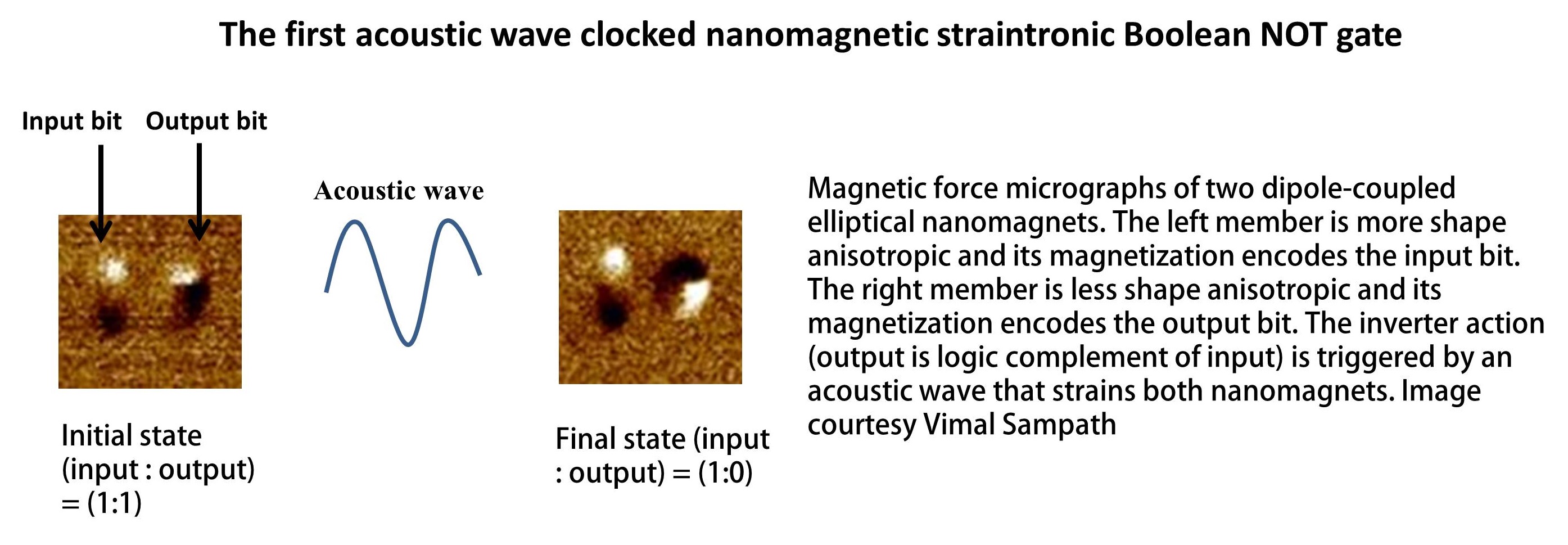
(2014) First experimental demonstration of logic gate functionality in magnetostrictive
nanomagnet arrays clocked with mechanical strain and successful information propagation with Bennett
clocking (Work performed in
collaboration with Prof. Jayasimha Atulasimha in the Department of Mechanical and Nuclear
Engineering at VCU).
(2015) First experimental demonstration of reversible magnetization switching in FeGa nanomagnets of ~250 nm
feature size on PMN-PT substrates due to electrically generated mechanical strain. First viable straintronic
non-volatile memory. Write energy dissipation is estimated to be ~2 aJ (Work performed in
collaboration with Prof. Jayasimha Atulasimha in the Department of Mechanical and Nuclear Engineering at VCU).
(2016) First experimental demonstration of magnetization switching in Co nanomagnets with surface acoustic wave.
(Work performed in
collaboration with Prof. Jayasimha Atulasimha in the Department of Mechanical and Nuclear Engineering at VCU,
Profs. Gary Atkinson and Umit Ozgur in the Department of Electrical and Computer Engineering at VCU).
(2016) First experimental demonstration of a micron-scale straintronic magneto-tunneling junction (Work performed in
collaboration with Prof. Jayasimha Atulasimha in the Department of Mechanical and Nuclear Engineering at VCU and Prof. Jianping
Wang in the Department of Electrical Engineering at Univ. of Minnesota).
(2016) First experimental demonstration of magnetization switching in super-paramagnetic Co nanodots by engineering
strain anisotropy (Work performed in
collaboration with Prof. Jayasimha Atulasimha in the Department of Mechanical and Nuclear Engineering at VCU and Prof.
Greg Carman in the Department of Mechanical and Aerospace Engineering at UCLA).
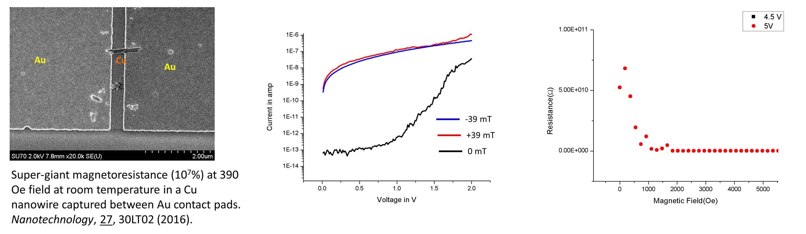
(2016) Discovery of a super-giant magnetoresistance (10,000,000% at room temperature) in copper nanowires
captured between gold contact pads with dielectrophoresis. The magnetoresistance accrues from Hall effect
modulation of potential barrier heights at Cu/Au interface (Work performed in
collaboration with Profs. Arunkumar Subramanian and Jayasimha Atulasimha in the Department of Mechanical and Nuclear
Engineering at VCU).
(2016) First experimental demonstration of complete magnetization reversal (1800 rotation of magnetization) in an
elliptical magnetostrictive nanomagnet due to strain. This challenged the traditional belief that strain can rotate the
magnetization of an elliptical nanomagnet by only up to 900. The 1800 rotation enables straintronic non-volatile memory.
(Work performed in collaboration with Prof. Jayasimha Atulasimha in the Department of Mechanical and Nuclear Engineering
in VCU).
(2017) Theoretical proposal for a precessionally switched voltage controlled perpendicular magnetic anisotropy
based magneto-tunneling junction (p-MTJ) that does not require a magnetic field. By using a magnetostrictive soft layer
and strain which replicates the effect of a magnetic field, precessional switching is obtained without a magnetic field.
(2018) First experimental demonstration of sub-nanosecond response time of a nanomagnet’s magnetization to acoustic
excitation generated in a piezoelectric substrate by ultrashort laser pulses (measured with time resolved magneto-optical
Kerr effect microscopy). (Work performed in collaboration with Prof. Anjan Barman of the S. N. Bose National Center for
Basic Sciences, Kolkata, India).
(2019) Demonstration of surface acoustic wave induced "simulated annealing" in an array of dipole coupled nanomagnets
fabricated on a piezoelectric susbtrate.
(2019) Demonstration of a sub-wavelength acoustic antenna (made of magnetostrictive nanomagnets) actuated by the giant
spin Hall effect in a Pt nanostrip.