Hierarchical Design Using SDL and ADK
1. Create a symbol for the nor2 gate
In this lab, you will use the design of your CMOS NOR gate
to create an AND gate. This will show you how to do hierarchical designs
using SDL.
1.1 The first step is to create a symbol for the nor2
gate you did in the last lab, so go to your lab5 directory and start
DA:
>> cd egre429/lab5
>> adk_da &
1.2 Open the nor2 schematic and use the Miscellaneous->Generate
Symbol... menu item to bring up the Generate Symbol dialog
box. Select the Or Gate shape and click OK. When the symbol
comes up, modify it to make it a NOR symbol. The result should look like
this:
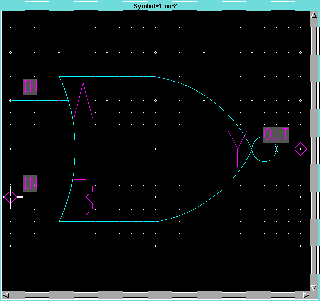
1.3 Check and Save the symbol and exit DA.
2. Create a hierarchical schematic for a 2 input AND gate using the
nor2 gates
2.1 Create a new directory for this lab and move into it. Start
DA:
>> cd ..
>> mkdir lab6
>> cd lab6
>> da &
2.2 Open a sheet called and2. Construct a schematic of a 2 input
AND gate using the symbol of the nor2 you just created in the lab5
directory. The result should look like this:
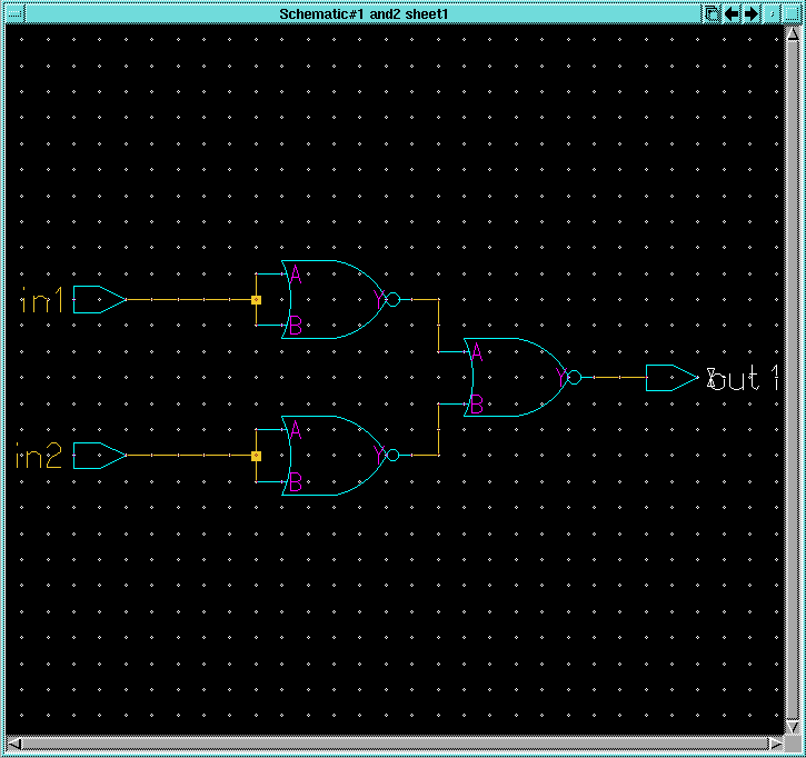
2.3 Check and save the sheet and exit DA.
2.4 You can functionally simulate your and2 schematic with Accusim,
just as you did for the nor2 gate. Don't forget to setup the analysis,
add forces, load the model library before you run the simulation. The result
should be a chart similar to this - its and AND gate!
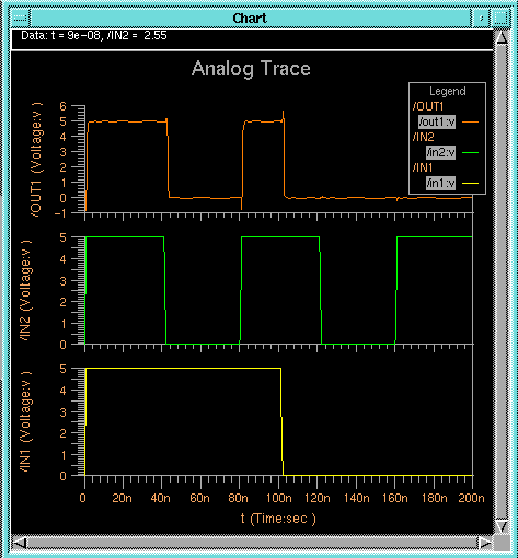
2.5 Exit Accusim.
3. Layout the hierarchical design in ICStation
3.1 Remember, before you can use SDL to create a layout from
a schematic, you have to run adk_dve on it:
>> adk_dve and2
3.2 Open ICStation and use
the Create button under the Cell menu in the Session
palette to bring up the Create Cell dialog box. Create a cell named
and2.
Remember to fill out the Process and Rules File
boxes and
select With Connectivity and select the sdl viewpoint for
the and2 schematic. Click OK. A new IC window should appear.
3.3 Click the DLA Layout button in the ICPalettes palette
and then click Logic > Open in the DLA Palette to bring up
the schematic of the and2.
3.4 Use the Setup->SDL... menu item to bring up the
Setup
SDL dialog box. When the Setup SDL dialog box appears, setup
the port styles as you did before by clicking on the SDL Port Styles
item in the Setup Values box and click the Setup... button.
Click the Process Port button in the resulting Set Active Port
Style dialog box and select the
default (width=4) item in the
Select
a Port Style box. Now, before you close the Setup SDL box, we
are going to setup the search path so that ICStation
can find the layout of the nor2 gate you did in the last lab. In
the Search Path box, type in the full pathname to the directory
where the nor2 gate layout is: /students/<your_id>/egre429/lab4.
Click OK in the Setup SDL dialog box
3.5 Now make the schematic window active and select the top left nor2
gate. Click on Place > Inst in the DLA Layout palette and
place the resulting symbol in the IC window. For some reason, the first
time or two you do this, you will get a default symbol that looks like
this:  . Simply
place it in the schematic, select it, delete it, and try again.
. Simply
place it in the schematic, select it, delete it, and try again.
After a few attempts, you should get the layout for the nor2
gate you previously created.
3.6 Select the bottom left nor2 gate and use Place > Inst
to place it in the layout. Place it directly abutting the other nor2
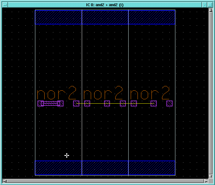
gate. Finally place the rightmost nor2 gate in the layout, but place
it at the same Y position, but to the right of the other cells, not touching
them. The result should be a layout like this:
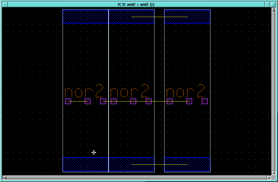
Notice how there are overflows for the connection between the nor2
gates, but also overflows for the connections between VDD-VDD and GND-GND
for the cells that are not directly abutting. For the cells that do abut,
the VDD-VDD and GND-GND connections are already made, so no overflows are
shown.
3.7 Select the rightmost nor2 gate and move it so that it abuts
the others. The VDD-VDD and GND-GND overflows should go away. Now all we
have to do is make the signal wire connections.
3.8 Finally, select the in1, in2 and out1 ports
one at a time and place them in the layout. Because they connect to one
of the ports in each nor2 gate, you can place them over the nor2
ports themselves and make the connection automatically.
4. Wire the hierarchical and2 gate.
Now we will wire the connections within the and2 gate
to match the schematic. You could do this manually using paths and shapes
as you've done before. If you opt for this route, remember that there is
a Metal1 blockage over all of the nor2 gates, so all routing
over the cells at this level must be Metal2 or higher. Also remember
that there are rules against stacking vias!
In order to illustrate its use, the ICStation
auto router will be used to route the interconnections here.
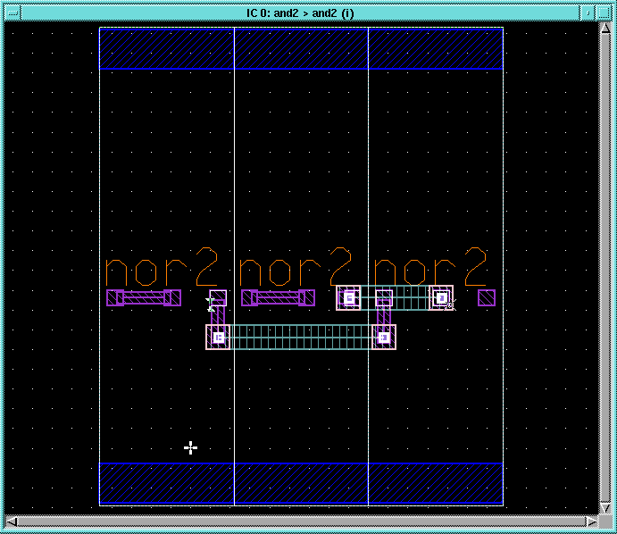
4.1 Select the overflow between the left most two ports on the nor2
gates. In the DLA Layout palette, click on the AutoR button.
When the prompt bar appears at the bottom of the screen, the Probe Extent
item will be highlighted. What the autorouter is asking you to do is specify
the area in the layout within which it can route the selected net. You
do this by drawing a box around the area where you would like the wire
to go with the left mouse button. Do that now by drawing a box around the
two ports where the selected overflow is connected. Magically, a Metal2
wire will appear between the ports and the overflow will disappear as below:
4.2 Select the overflow between the middle nor2 gate's inputs
(it may be easier to select it on the schematic) and autoroute that as
well.
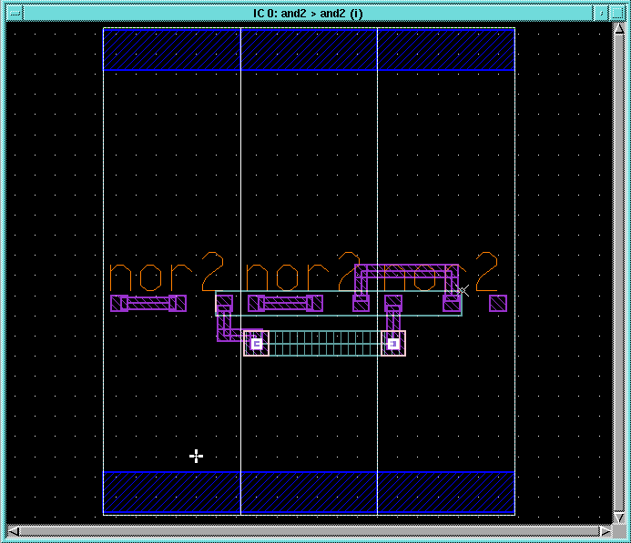
4.3 Select the connections between the output of the left nor2s
and the inputs of the right nor2 (this may be easier in the schematic
as well) and autoroute them. You'll have to give the autorouter a larger
area to work with, so draw the Probe Extent box larger in the Y
direction this time. If one or both of the routes does not get done, you
probably didn't draw the box big enough, so try again. The end result will
be something like this:
4.4 Do a DRC check at this time to see if the autorouting was done OK.
If you end up with a routing like the one above, you will get errors because
Via2
between Metal2 and Metal3 was placed above a
Via between
Metal1
and Metal2 by the autorouter. This was most likely caused
by it not seeing the Via inside the
nor2 cell. There are
several ways to fix this, but the easiest way is to add Metal3 blockages
over the Metal2 ports. This will cause the autorouter to use Metal2
to come out from over the ports before it uses Metal3 (and the associated
Via2s).
4.5 Make the IC window active and type undo in the window and
hit <Return>. Do this several times until the overflows you just
routed return. Unselect all and add a shape of METAL3_BLKG
around the remaining unrouted Metal2 ports at least one lambda outside
them. Make sure that the aspect is set to internal. Select
the two unrouted overflows and route them again. Hopefully, the result
will be something like the one below:
4.6 Do a DRC check of the design and you should have no errors.
Note that if we were going to use this cell at a higher level of hierarchy,
we would have to put Metal1 ports on it for VDD and GND, Metal3
blockages over the Metal3 routes within the cell, and an fp1
layer around the border of the cell. You can certainly use multiple levels
of hierarchy in your design, and this would help you manage complexity,
but it is not without its disadvantages.
4.7 Go to the ICtrace (M) palette and select LVS to do
a layout vs. schematic check. Select the sdl viewpoint for the and2
gate in the Source Name item of the LVS(Mask) dialog box
and be sure to turn off Recognize Gates as you did before. After
the LVS check is complete, use Report > LVS to view the report.
If you did not add the VDD and GND ports, you will get two errors for that,
but if you add these ports, the LVS check should come up with no errors
and only a few warnings. You should check the warnings to be sure that
they are ok, and in this case, they seem to be.
4.8 Close the LVS Report window.
5. Extract a netlist and do post-layout simulation with MachTA
5.1 Go to the ICextract (M) palette and click on Lumped.
Extract a netlist called and2.sp as you did for the nor2
gate. Be sure to set the ground name to GND. Save the and2 cell
and exit ICStation.
5.2 Fix the and2.sp file for simulation with MachTA:
>> cell_sim_prep and2
5.3 Start MachTA on the
fixed and2 Spice file:
>> mta -t $ADK/technology/mta/ami05
mta_and2.sp
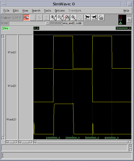
5.4 Plot v(in1), v(in2), and v(out1), force some values on the in1
and in2 signals and run the simulation. You should see a result
like this - its still an AND gate!
5.5 Exit MachTA.