1.1 Move into the directory you created for this class, create
a directory for lab 4, and move into it. Then start ICStation:
>> cd egre429
>> mkdir lab4
>> cd lab4
>> adk_ic &
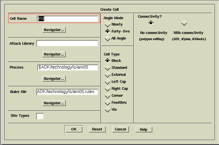
1.2 In the session palette window, click on CREATE with LMB (left
mouse button). Fill out the Create Cell dialog box like the one
shown below and click OK.
1.3 Create the power (VDD) and ground (GND) rails for the inv
cell by making the IC window active, placing the cursor in the IC window
and typing pwr(). You should see the rails appear with N_Well
and P_Well above and below them in the proper spot. Note that the
pwr()
command is just a macro that has been provided for you to make layout easier.
This macro places Metal1 in the proper places for VDD and GND, makes
them ports with those names, and places the N_Well and P_Well.
You can move or resize the resulting structures to match any cell width
or height you desire.
ICStation has
a feature called device generators built into it that can layout a structure
automatically for you. Device generators are a lot like the pwr()
macro you used above except that they create a separate design unit, almost
like another cell, that gets instantiated into your layout. The ADK design
kit has device generators for NMOS and PMOS transistors which we will use
for this design.
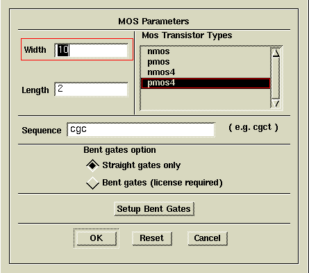
2.1 Click on the DLA Device item in the IC Palettes palette
and click on AddMos in the DLA Device palette. Select the
pmos4
device and set the width to 10 (which means 10 lambda units)
and length to 2 (remember, length is always 2 lambda for
a standard CMOS transistor!). The sequence parameter tells the device
generator what combination of polysilicon gates and contacts you want in
the transistor. For this transistor, the default cgc, which means
contact-gate-contact
is what we want. For a diffusion shared string of three transistors the
sequence would be cgggc meaning
contact-gate-gate-gate-contact.
You can have any arbitrary sequence of gates and contacts and also specify
a different width for each transistor by putting a comma separated list
of numbers in the width field.
When you have the MOS Parameters dialog box setup like the one
below, click OK.
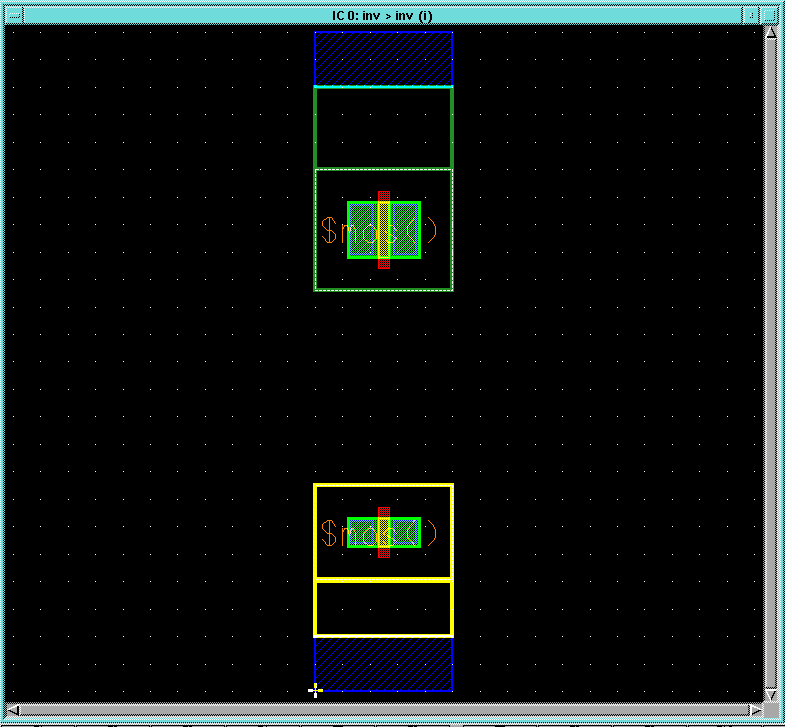
2.2 Click the LMB in the cell window near where you want the PMOS transistor
and when it appears, move it so that the upper left-hand corner of the
N_WELL
surrounding it lines up with the corner of the N_Well under the
VDD rail.
2.3 Click on AddMos again and select the nmos4 device
with a width of 5, a length of 2, and a sequence of cgc
in the MOS Parameters dialog box and click OK.
Place the resulting NMOS transistor next to the P_WELL above the GND rail.
The resulting layout should look like the one below.
Note that only part of the transistor layout within the MOS device is
shown at this level. There are N_PLUS_SELECT, P_PLUS_SELECT,and
CONTACT_TO_ACTIVE
shapes inside these devices that make them complete transistor layouts.
If you want to see what is inside a MOS device, select it (the $mos()
lable
will turn white when the entire device is selected) and use the
Context->Hierarchy->Peek
item from the pull down menu to bring up the Peek dialog box. Set
the Number of Levels item to 1 and click OK. You will
then see all of the layers in the MOS device. To go back to the external
view of the MOS device, select it and use the
Context->Hierarchy->Unpeek
menu item.
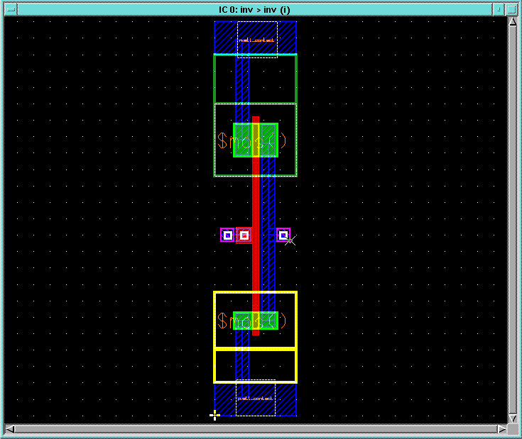
2.4 Use your skills in ICStation
to complete the layout so that it looks like the one below. Don't forget
to put a Metal2.port on the input and output and make the input
a port with the name in1 and the output a port with the name out1.
The pc() macro is handy for adding poly contacts and the nwc()
and pwc() macros are handy for adding N_WELL and P_WELL
contacts. Do a DRC check on the cell and fix any errors that are listed.
ICStation has
another feature called LVS (layout vs. schematic) that can check a layout
and compare it against a transistor level schematic. We will use this capability
to check your layout against the inverter schematic you created and simulated
in lab1.
3.1 Go back to the IC Palettes in the palette menu and click
on ICtrace (M). In the ICtrace (M) palette, click on LVS.
3.2 In the LVS (Mask) dialog box under the Source Name...
item, click on Navigator. Navigate up to your egre429 directory
and down into the lab1 directory. Go into the inv directory
and select the sdl viewpoint by clicking on the  item. Click OK in the Navigate dialog box to close it Click on the Setup
LVS... button in the LVS (Mask) dialog box and set the Recognize
Gates item to NO in the Setup LVS dialog box that comes
up. Click
OK in that dialog box and OK in the LVS (Mask)
dialog box. A number of messages will flash by at the bottom of the ICStation
window with "Mask results database loaded" as the last one.
item. Click OK in the Navigate dialog box to close it Click on the Setup
LVS... button in the LVS (Mask) dialog box and set the Recognize
Gates item to NO in the Setup LVS dialog box that comes
up. Click
OK in that dialog box and OK in the LVS (Mask)
dialog box. A number of messages will flash by at the bottom of the ICStation
window with "Mask results database loaded" as the last one.
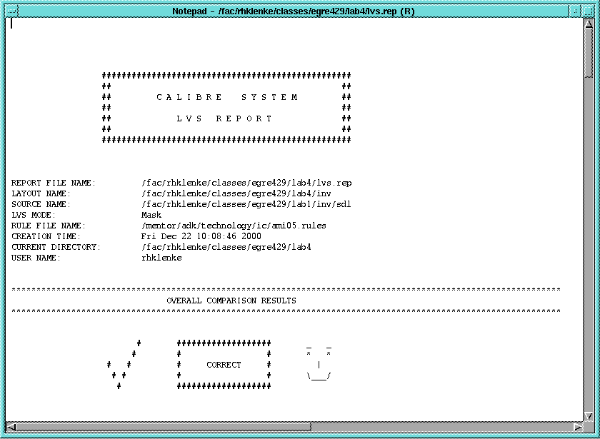
3.3 To view the LVS results, select the Report item from the
ICtrace
(M) palette and select the LVS item from the popup menu that
appears. The result should be a report window with the infamous "smiley
face" as shown below:
You can now use the ICextract (M) tool in ICStation
to extract the spice netlist and simulate it with MachTA
as you did in lab3.