Accusim is the Mentor
version of the Spice simulator and works much like PSpice that you
are familiar with. We can use the transient analysis mode to simulate the
function of the circuit to ensure that it is performing correctly.
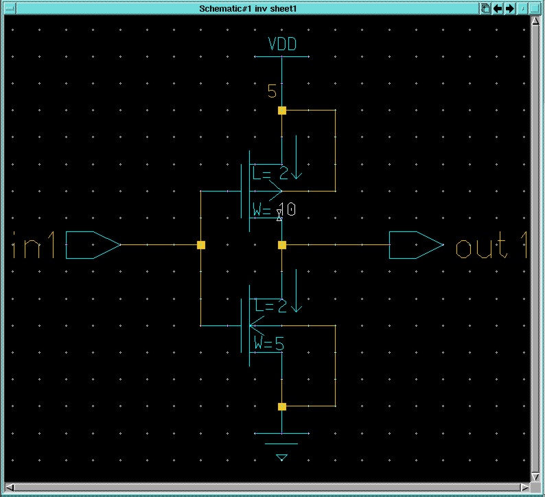
1.1 Create an Accusim
viewpoint for your inverter design:
Note that this viewpoint is created inside the inv directory
so you will not see it and this command also creates other viewpoints that
you will use later for LVS and SDL.
1.2 Invoke Accusim on
your inverter design:
This will bring up the Accusim
window shown below:
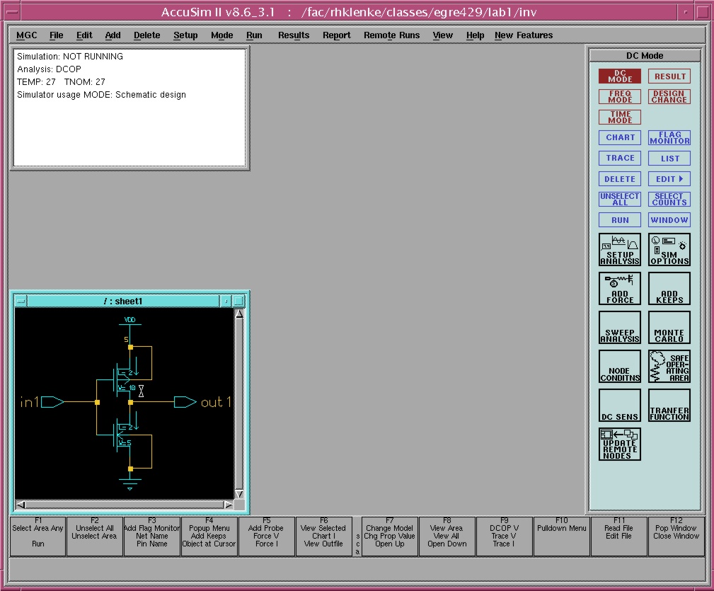
1.2 Once Accusim is loaded, you should see your schematic. The
first thing that we need to do is to set up the analysis type. Do this
using the Setup Analysis icon in the palette menu. Since you will
be performing a transient analysis, you need to press the Transient
button to get the dialog box for setting up a transient analysis. You should
use a time step of 1 ns and a stop time of 500 ns. Leave everything else
at its default value. The dialog box should look like this when you are
done:
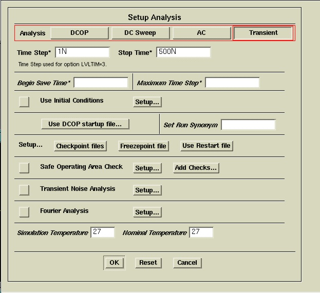
Click the OK button to exit the dialog box.
1.3 Next, you need to set the input forces. Select signal in1
and then use the Add Force icon or menu to add a force. This should
be a pulse type force with an initial value of 0 V and a pulsed value of
5 V. The pulse width should be 200 ns with no delay and a period of 400
ns. The Add Force dialog box should look like this:
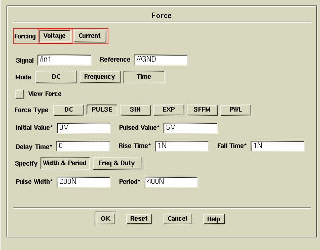
Note that the signal that you selected is listed as is the //GND
as a reference. Click OK when done.
1.4 To trace the input and output values, select both the in1
and the out1 signals and press the trace button on the
palette menu. A chart window with an Analog trace of both signals will
open.
1.5 Before you can run the simulation, you must tell the simulator what
the models are for your FETS. The model names are "tp" and "tn" for the
P- and N-FETS, respectively. There is a model file in $ADK/technology/accusim/ami05.mod
that you can use for the AMI 0.5 micron process To load a model file, use
the File->Auxiliary Files->Load Model
Library menu. You can then enter the filename with your models in
it. Use the navigator to go to the $ADK directory and navigate into
the technology/accusim directory. Load the above file and click
OK.
1.6 Now type run in any window to run the simulation (or use
Ctrl-F1).
The result should be a chart of the values on in1 and out1
as shown below.
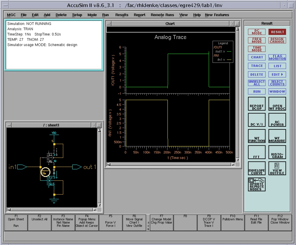
1.7 Make the chart window active and print it using the File->Print->Active
Window... menu item. Exit Accusim.
Like PSpice, Accusim can be used to perform other analysis
as well. Here we will examine the voltage transfer characteristic of the
inverter using Accusim.
1.1 Restart Accusim on your inverter:
>> accusim inv/accusim
&
1.2 Select the in1 signal and THEN press the Setup Analysis
icon in the palette menu. Press DC Sweep and notice that the Positive
Net and Negative Net are already set to /in1 and /GND already.
Set the From and To values to 0V and 5V respectively. The result should
be a dialog box like this:
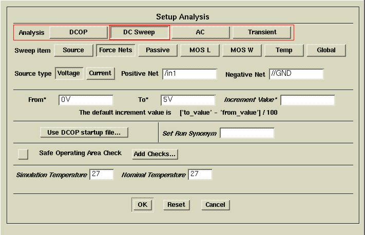
Click OK when you are done.
1.3 Trace the in1 and out1 signals and load the ami05
model file as before and type run in the window to run the simulation.
The result should be a chart window like that shown below:
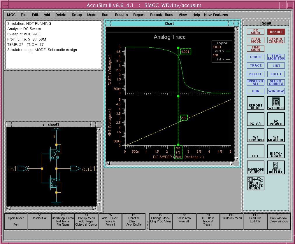
1.4 Print the chart window and exit Accusim.
Based on the tutorial prepared by David Zar.