PLDS II and BP1400 Universal Device Programmer
1. What you will learn
1.1 How to export a schematic drawn in Design Architect to PLDS II.
1.2 How to set design parameters (such as manufacturer and package type)
in PLDS II.
1.3 How to generate a fuse map file for the schematic and parameters
selected.
1.4 How to redraw the schematic in DA using the PAL.
1.5 How to set the PAL fuse map reference file.
1.6 How to change the pinout of the PAL by altering the ".pi" file.
1.7 How to FTP a file from the UNIX lab to a PC.
1.8 How to program a PAL using the BP1400.
2. Create the schematic and symbol for the PLDS II device
The logic design to be mapped into a PAL with PLDS II is created
by developing a schematic of the logic using parts from the Mentor gen_lib
library.
This schematic is then exported to the PLDS II tools. Note that the schematic
can be developed by hand in Design
Architect or synthesized to gen_lib parts from a VHDL
model using the Mentor Graphics Autologic
synthesis tool.
2.1 Create a tutorial directory under your root directory and start
Design
Architect (DA) in it:
>> cd egre427
>> mkdir tut
>> cd tut
>> da &
2.2 Open up a new sheet for this design and call it pal1.
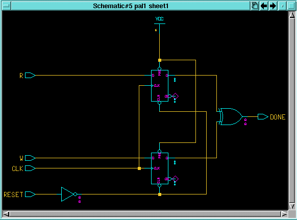
Construct the schematic shown below using only gen_lib parts:
2.3 Check and save the sheet.
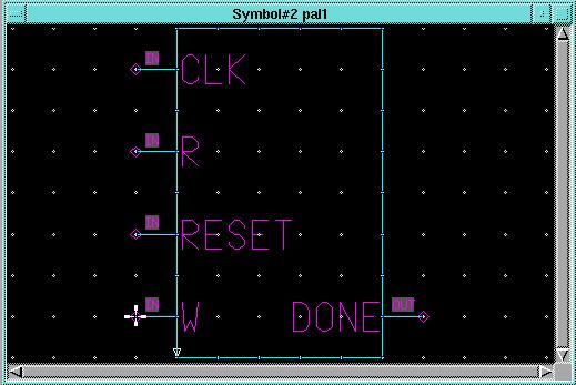
2.4 Create a symbol like the one below using the Miscellaneous->Generate
Symbol menu item.
2.5 Check and save the symbol. Close the symbol window. Leave the DA
and the pal1 schematic open.
3. Check the schematic in Quicksim
3.1 Copy the do file:
>> cp /mentor/examples/quicksim/pal1.do
.
3.2 Open Quicksim:
>> quicksim pal1 &
3.3 Run the dofile by typing "dofile pal1.do" in the session window.
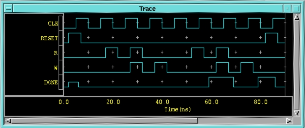
The resulting timing diagram should look like the one below:
3.4 Exit Quicksim.
4. Export the schematic to PLDS II and Generate the Fuse (JEDEC) File
4.1 Back in DA, make
the schematic window active and select File->Export
to PLDS II. After a moment, a PLDS II window similar to the
one shown below will appear.
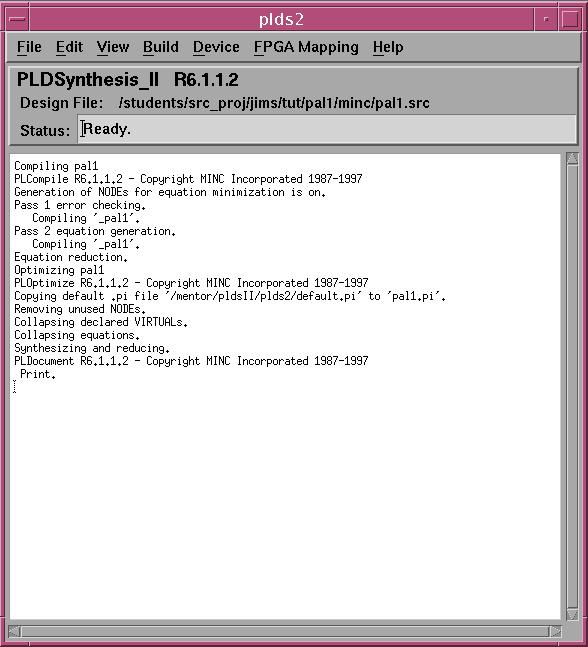
4.2 In the PLDS II window, select the Build->Build
Design menu item. A number of messages will be printed in the
window, but no errors or warning should occur.
4.3 Select the Device->Parameters->Contraints
menu item in the PLDS II window. The prompt box shown below will appear.
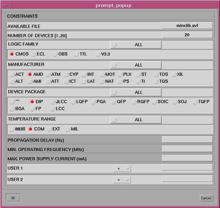
4.4 Under LOGIC FAMILY select CMOS. For MANUFACTURER
select AMD. Under DEVICE PACKAGE select DIP. Finally,
for TEMPERATURE RANGE select COM (commercial.) Click OK.
4.5 Select the Device->Parameters->Templates
menu item. The prompt box shown below will appear.
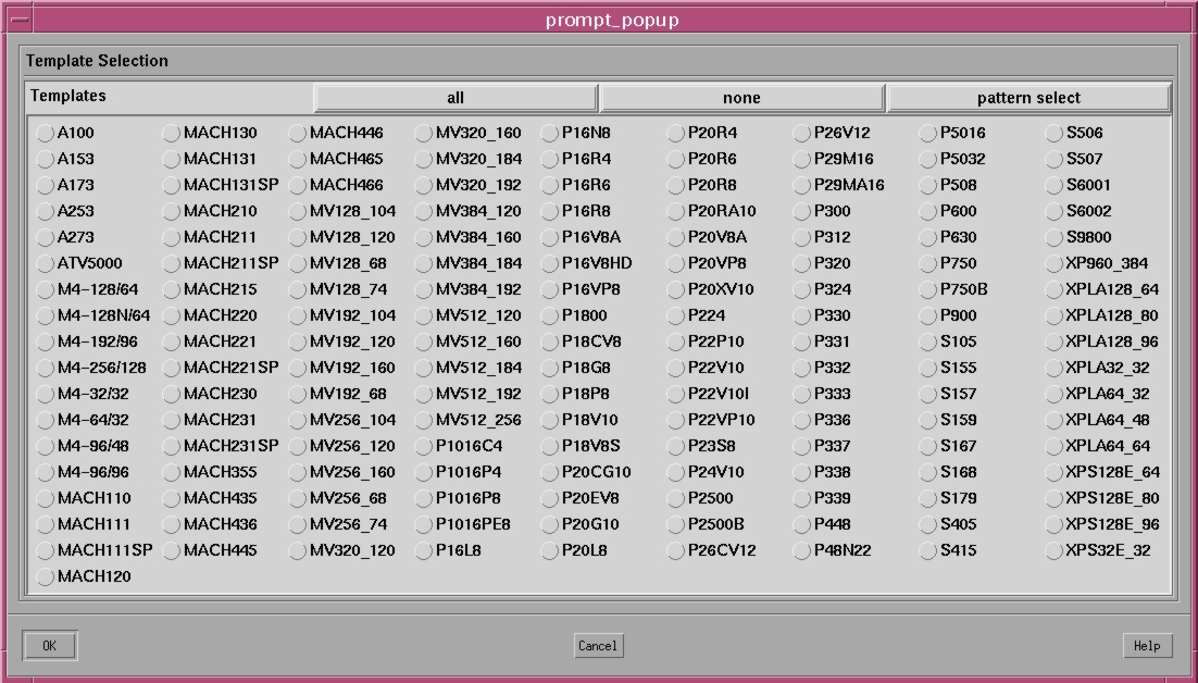
4.6 In this box, click the none button to unselect anything that
may be selected. Next, select P22V10. Click OK.
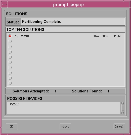
4.7 In the PLDS II window, select the Device->Solutions->Generate
New Solutions menu item and the prompt box shown below will
appear. Click OK.
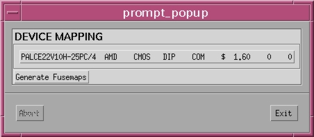
4.8 Finally, in the PLDS II window, select the Device->Device
Mapping menu item and the prompt box shown below will appear.
Click Generate Fusemaps and then Exit.
4.9 Note that if you select the View->Documentation
menu item in the PLDS II window, you will see info about the programmed
PAL, including a pinout which should look like the one below:
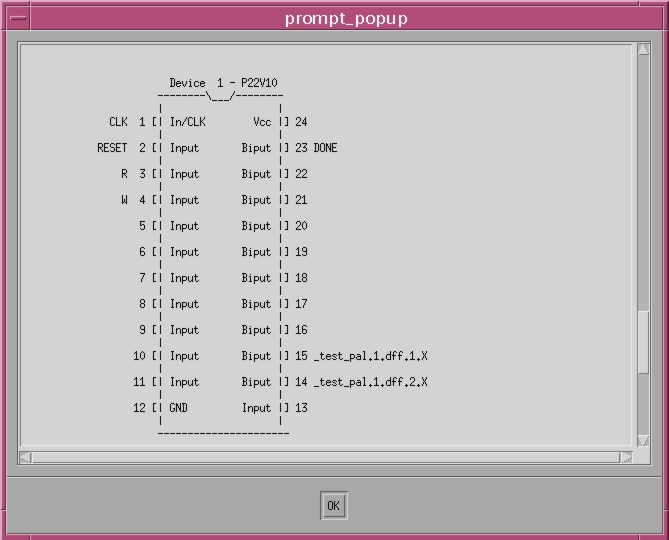
4.10 Click OK in the documentation window and use the File->Exit
menu item to exit PLDS II.
5. Redraw the schematic in DA using a 22V10 PAL model
Once you have generated a JEDEC fuse file for the PAL, you
can simulate it in a 22V10 model in your original system model to ensure
that the PAL will perform as expected in the real system. This is done
using a 22V10 model available within the Mentor Graphics library and setting
it up so that it loads the JEDEC file you generated in PLDS
II.
5.1 Start DA and open
a new sheet called pal2.
5.2 Get a 22V10 component by opening the Board Process library using
the Libraries->MGC Board Process Libraries
menu item and selecting the PLD option from the MGC BPL Libraries
sidebar menu. Click once on the 22V10_10 option in the dialog box
that appears. Click the Refine Component button. In the Symbol
item, select GRAY_BOX. In the Package item, select DIP24_P.
Click OK and place the symbol on the schematic.
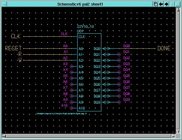
5.3 Using this symbol, draw the following schematic in DA:
5.4 The filename located below the symbol must be changed. This
filename must be the pal1.j1 file (called a "JEDEC" file) created
when you generated the fusemap in the PLDS II window. This file is located
in the "minc" directory created by PLDS II under the directory you created
earlier in the tutorial (e.g:students/<your_id>/egre427tut/minc/pal1.j1)
To change this filename, simply position the mouse pointer over the filename
that appears just below and to the left of the PAL symbol on the schematic
and press <Shift-F7>. In the box that appears, write in the
complete directory for the filename.
5.4 Check and save the schematic.
6. Check the schematic in Quicksim
6.1 Open Quicksim
>> quicksim pal2 &
6.2 Open sheet and run the simulation by typing "dofile pal1.do" in
the session window. The resulting trace window should look the same as
that for the pal1 schematic.
6.3 Exit Quicksim.
7. (Optional) Change the Pinout of the PAL
There may be occasions where you need to make a minor change to a
PAL that is already in a prototype board and you do not want to rewire
the board to accommodate the new PAL. In this case, you need to have PLDS
II configure the new PAL so that it has the same pinout (signal
name to device pin mapping) as the old PAL. This portion of the tutorial
explains how to do that.
NOTE: If you are using this tutorial only to generate a fusemap file
for the "Test Board," do not do this part of the tutorial unless afterwards
you change the pal1.pi back to its original form and regenerate the original
JEDEC file . The PAL socket on the test board is wired for the original
PAL pinout.
7.1 The PLDS II tool
automatically assigns the location of the pins on the PAL device, but sometimes
it is desirable to assign the pin locations yourself. In order to do so,
the pal1.pi file must be edited.
7.2 Open a text editor, and open the pal1.npi file (not the pal1.pi
file). This file is located in the "minc" directory along with the JEDEC
file created above. (For example: /students/<your_id>/egre427/tut/pal1/minc/pal1.npi)
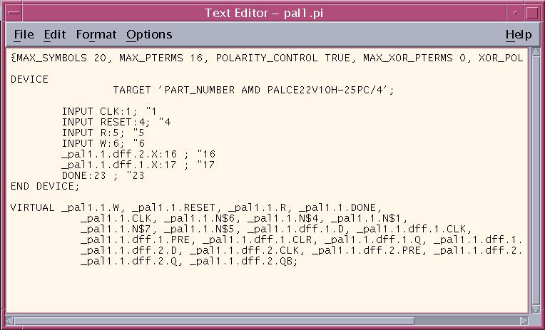
The file will look similar to the one below.

7.3 The section of the file we are interested in is between the
"DEVICE" and "END DEVICE;" labels. To change which pins to assign inputs
and outputs to, this part of the file will be altered. Change the line
reading INPUT RESET:2; "2 to INPUT RESET:4; "4.
This will move the RESET input from pin 2 to pin 4. Similarly, change the
rest of that section of the file to look like the file below. (Pin 1 is
a dedicated clock input, which will not be altered.)
7.4 In the text editor, save the file. Also, save the file as pal1.pi.
7.5 Reopen the pal1 schematic in DA.
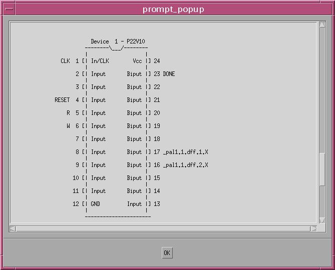
Perform steps 4.1 to 4.9 again. Note the pinout of the PAL as shown in
the documentation file looks like the one shown below.
7.6 Exit PLDS II and DA.
8. Program the Actual PAL
8.1 On the computer connected to the BP1400 in
room 211, you will need to create your own subdirectory which will have
the same name as your user name (if you have not already done so.) Your
user name is the same as your login (e.g: s2joshmo). Open a DOS window
and type the following:
>> cd\
>> cd students
>> mkdir <user name>
>> cd <user name>
8.2 Keep the DOS window open. Stay in your student directory. In order
to program the PAL, the JEDEC file generated above will have to be copied
to the computer connected to the BP1400. The easiest way to do this is
by using FTP. At the DOS prompt type the following:
>> ftp vlsi01.egr.vcu.edu
You will be prompted for your login name and password for the SUN lab.
Once you are logged in type:
>> binary
The prompt should say "Type set to I." Now you will want to cd into the
directory where your JEDEC file is on your UNIX account.
>> cd egre427/tut/pal1/minc
The prompt should say "CWD command succesful." Now, to get the JEDEC file,
type:
>> get pal1.j1
The prompt should say "Binary Transfer complete." Now quit ftp:
>> quit
You should now be returned to the DOS prompt. Type "exit" at the prompt
to close the DOS window.
8.3 Now you will need to start the "BP" program which controls
the BP1400 programmer. First, make sure the proper module is on the BP1400
and that no chips are in the zero insertion force socket. Turn the BP1400
on, and wait until only the green LED is lit.
8.4 On the desktop of the computer connected to the BP1400, double click
on the BP icon to start the program. Wait for the program to finish
establishing communication with the programmer before you proceed to the
next step.
8.5 Before you can program a chip you must select a device to program
and load data into the programmer's buffer.
8.6 To select a chip, choose the Select submenu from the main
menu. (There is no mouse, so use the arrow keys or press the first letter
of the menu item you want; once highlighted, press enter.) Type
in PALCE22V10H-25/4 if it is not already selected. Press the enter
key. The chip should now be selected.
8.7 To load the buffer, choose Buffer/Load from the main menu.
Type in the directory where the JEDEC file is located, followed by "*.j1"
(e.g: C:/students/s2joshmo/*.j1). Select your file in the list of
files that appears and press return. Make sure that JEDEC is highlighted
in the Type field and press return.
8.8 After putting on a grounded wrist strap, carefully remove a PAL
device (numbered PALCE22V10H-25PC/4) from its package and place it in the
zero insertion force socket. Make sure the dot on the corner of the chip
is at the upper right, and the device is all the way at the top of the
socket.
8.9 Choose Device/Program from the main menu and press return.
The yellow "active" LED will light while the device is programming. A short
high pitched beep will be heard when the device is finished programming,
and the green "PASS" LED will light. After the device is programmed, remove
it from the zero insertion force socket. It is now ready to be inserted
into the test board.
You have completed the PLDS II tutorial.