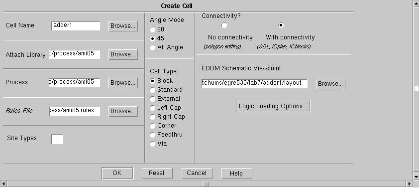
2.1 Click on
Floorplan in the
IC
Palettes palette. In the
Floorplan palette, click
Autofp.
Leave the default setting in the
Autofloorplan Options dialog box
that pops up and click
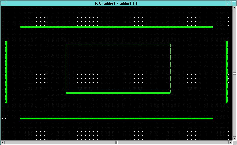
OK. This will result in a set of floorplan
shapes being added to the
adder1 window which specify the rows into
which the standard cells that make up the
adder1 component will
be placed and the external edges of the block onto which the ports will
be placed. The
adder1 window should look like the one below:
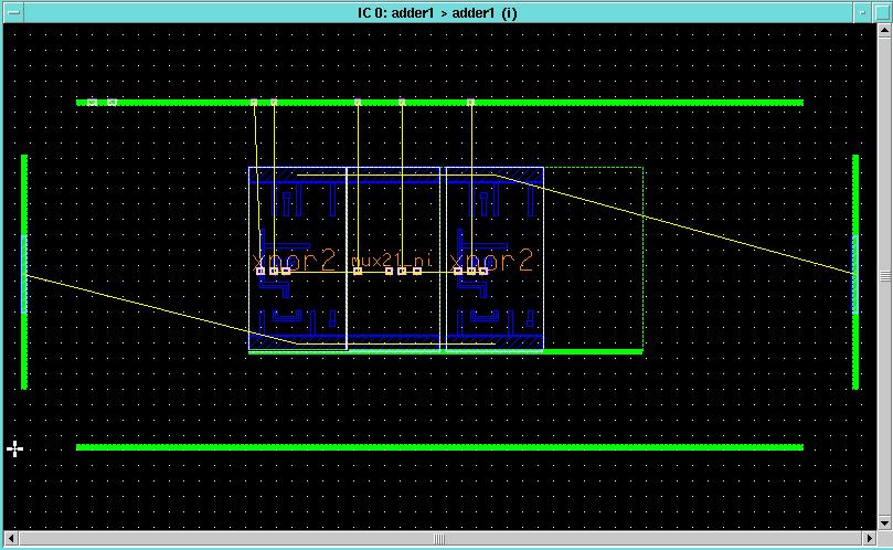
2.2 Click Back in the Floorplan palette and click
Place
& Route in the IC Palettes palette. In the
Place
& Route palette, click StdCel under the Autoplc item.
Leave the default options set in the dialog box that comes up and click
OK.
Next, click Ports under the Autoplc item. Leave the
defaults checked in the dialog box that pops up and click OK.
The result should be an adder1 window that looks like this one:
2.3 From the Place & Route palette select All
under the Autorou item. The AUTOROU AL dialogue box will appear
as shown.

2.4 Click Options in the Autoroute All dialog box
that comes up. The Autoroute All Options dialogue box will come up
as shown.
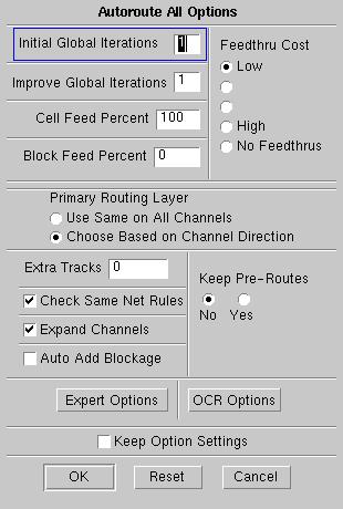
2.5 In the Autoroute All Options dialog box, click Expert
Options. The Router Expert Options dialogue box will come
up as shown.
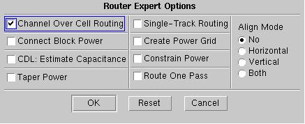
2.6 Select Channel Over Cell Routing and click OK
in the Router Expert Options dialog box that comes up. Click
OCRoptions
back in the Autoroute All Options dialog box. The OCR
Options dialogue box will come up as shown.
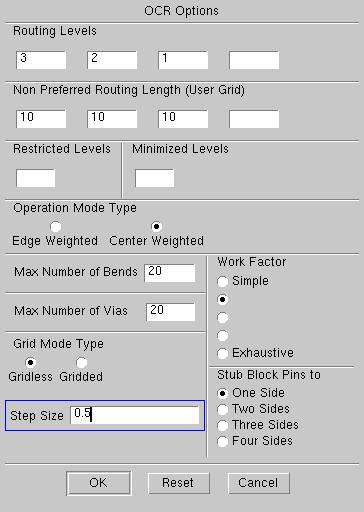
2.7 Set the step size to .5 and the
Operation
Mode Type to Center Weighted and click OK in the OCR
options dialog box. Finally, click OK in the Autoroute
All Options dialog box and the Autoroute All dialog box to begin
routing. Depending on the size of the design this may take several
minutes. When the process has completed the mouse pointer changes
back from an hourglass to an arrow and the results of the process are in
the transcript. The result should be an adder1 window that
looks like the one below (you may need to press Shft-F8 to zoom
all):
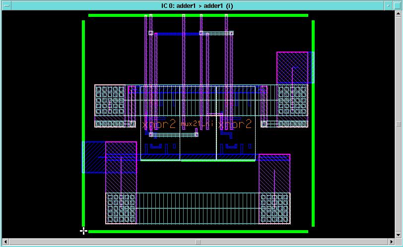
This small design will route completely the first
time. However, for large designs, some un-routed overflows may still
exist. These overflows must be routed as described below:
This step is necessary even if overflows don't immediately appear in
the routed layout. When zoomed out small overflows may not be viewable,
but may still exist. To select all overflows in the design type "check
over". In the form window that appears select All and OK
the form. Next, from the Place & Route palette select Overflw.
If the response "An object of type Overflow must be selected" appears in
the status block, there are no overflows to route. Otherwise, the overflows
will be routed.
2.8 One little caveat with the tools that must be fixed AFTER autorouting
(else the autorouter crashes IC Station): Autoplacement of
ports only makes the METALx layers for the ports. You can easily
fix this by manually adding METALx.PORT over each of the ports. Also,
remember the Calibre PEX tool requires the port name text be associated
with the METALx.PORT shape for each port. You will add the text for
all port names after you have added the METALx.PORT shapes for each port.
Here are the steps for each port:
-
Unselect everything (F2) then select a port (make sure you select
a port by checking the transcript in the lower left corner)
-
Use Easy Edit to add a shape of the corresponding METALx.PORT
(Aspect=Both)over the exisiting METALx (you do
not have to cover it completely)
-
Press Esc to terminated adding shapes
-
While both shapes are still selected, choose Connectivity->Port->Add
to Port to connect the METALx.PORT shape to the existing
METALx port
-
Repeat for all ports (each connection on the outer ring is a port)
Once you have finished adding the METALx.PORT shapes and connecting them
to the ports, then unselect everything (
F2) and choose
Objects->Add->Add
Text on Ports to associate the port name text with the ports.
2.9 Run DRC and fix any errors manually. At this
time you should be able to run LVS and ensure the layout is correct.
Also you should be able to perform a Calibre PEX extraction then
simulate with MachTA to ensure your design will work.
2.10 Save the layout by selecting File->Cell->Save Cell->Current
Context. You may save the layout and exit the IC Station
session at any time. To re-load the layout later, choose open from
the IC station palette. If you wish to make changes to the cell,
you must also selectFile->Cell->Reserve Cell->Current Context.