5.1 Select
File->Import Verilog...
from the top menu bar. You will see a dialogue box as shown below.

This dialogue box has one strange property - whenever you click the
Netlist
File(s)... button or the Output Directory... button or the Mapping
File(s)... button it opens the same dialogue box. A little confusing
if you are not expecting it...
5.2 You will need to fill out all three of the top fields.
Click on the Netlist File(s)... button (or either of the other two)
to show the following dialogue box. Note the slider scroll on the
bottom of this dialogue box - this box is wider than will show in the default
DAIC
window.

5.3 Fill in the Netlist File(s) file list by first
highlighting the adder1.v file in the left file list then
clicking the Add-> button for the top right file list.
5.4 Fill in the Output Directory file list by first
left clicking on the BrowseUp (yellow folder with the up arrow in
it) then highlighting lab7 in the left file list then left
clicking the Add-> button for the middle right file list.
5.5 Fill in the Map File(s) file list by navigating
to the /mentor/adk3_0/technology directory, highlighting
the adk_map.vmp file in the left file list then left clicking
the Add-> button for the lower right file list. Your dialogue
box should look as shown.

5.6 Click OK for this dialogue box then OK for the
Import
Verilog dialogue box. DAIC will begin importing the design from
your Verilog gate level netlist. When it completes, you will see
the following message in the lower left status line:

5.7 Open the schematic for adder1 by left clicking on the Schematic
button in the Open portion of the session palette.
You will notice DAIC has created a component for adder1.
Double click on it, highlight the schematic and click OK.
Click OK again to open the schematic. You schematic should
look something like:

5.8 Click on the session button in the right palette. Then
click on the Symbol button in the Open portion of the schematic and open
the symbol as you did the schematic. Your symbol should look something
like:

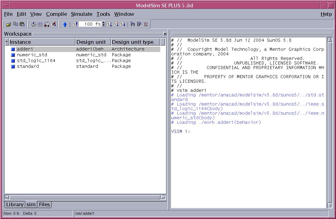
5.9 Close the symbol window. Simulate the schematic as you
have done in previous labs. There is one difference now: your schematic
has a lot of properties not normally associated with schematcis.
So when you are setting up the simulation, you should not check the Automatic
check design before netlist option in the Setup Simulation Environment
dialogue box.

5.10 Close the EZ wave viewer. End the simulation.
Now you are in familiar territory - just click on the Prep for Layout
button as before and wait for the prep to complete. Then exit DAIC.