Hierarchical Design Using SDL and ADK
1. Create a hierarchical schematic for a 2 input AND gate using
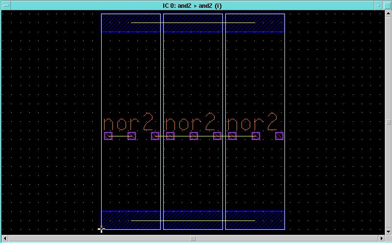
the nor2 gates
1.1 Create a new directory for this lab and move into
it. Start
DAIC:
>> cd egre533
>> mkdir lab6
>> cd lab6
>> adk_daic &
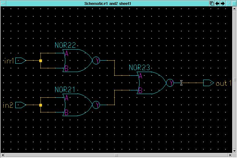
1.2 Open a sheet called and2. Construct a schematic
of a 2 input AND gate using the symbol of the nor2 you just created
in the lab5 directory. Use the Add Instance button in the schematic
edit palette to add your nor2 gates to the schematic. Use the ADK
IC Library parts for in and out ports. Check and save your schematic,
fixing any errors. The result should look like this:
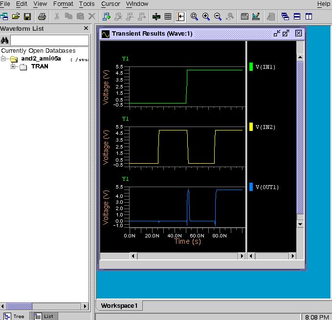
1.3 Simulate your and2 schematic with ELDO, just
as you did for the nor2 gate. The result should be a chart
similar to this. Note now with two levels of hierarchy some of
the non-ideal effects are showing up. You can see a spike caused
by the finite rise and fall times on the inputs. Close the waveform
viewer. Close the simulator by pressing the end simulation
button.
Remember the problem with DAIC - you must exit then
restart after simulating!!!
1.4 Close DAIC. Start DAIC again from the
Unix command window (adk_daic &). Open your and2
schematic for editing.
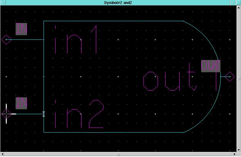
1.5 Create a symbol for the and2 schematic - as you did in lab5
except this time pick an AND gate body. Your symbol should look like
the one below. Check, save and check the symbol then exit the symbol
editor. Check and save the schematic. Prepare the schematic
for layout (click the Prep for Layout button). Exit DAIC.
2. Layout the hierarchical design in ICStation
2.1 Remember, before you can use SDL to create a layout
from a schematic, you have to run adk_dve on it to create a layout
viewpoint:
>> adk_dve and2
2.2 After adk_dve completes, open ICStation
and use the Create button under the Cell menu in the Session
palette to bring up the Create Cell dialog box. Create a cell named
and2.
Remember to fill out the Process and Rules File
boxes and
select With Connectivity and select the layout viewpoint
for the and2 schematic. Click OK. A new IC window
should appear.
2.3 Select Context->Set Cell Config->Connectivity Editing
from the top menu bar. ALWAYS DO THIS WHEN USING SCHEMATIC DRIVEN
LAYOUT!!! Also remember to change the SnapX and SnapY
values to 0.5 under Other->Window->Set Grid.
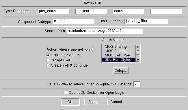
2.4 Select Setup->SDL from the top menu bar.
This time you must supply a Search Path to the nor2 layout
you created in lab5 (students/your_name/egre533/lab5).
As before, setup the SDL Port Styles to Connect Layers, METAL2.PORT,
width=height=4. Your completed dialogue box should look similar to
the one below:
2.5 Click the DLA Layout button in the ICPalettes
palette and then click Logic > Open in the DLA Palette to
bring up the schematic of the and2.
2.6 Now make the schematic window active and select the top left
nor2
gate. Click on Place > Inst in the DLA Layout palette
and place the resulting symbol in the IC window. As before you will
get the little placeholder shown below:

Simply place it in the schematic, select it, delete it, and try again.
The second time you should get the full sized layout of a nor2 gate
you previously created. Place it in the IC layout window. Then
select the bottom left nor2 gate from the schematic and place it
in the IC layout window to the right of the first nor2 gate but
not touching. Finally select the third nor2 gate (output
gate) and place it to the right of the second nor2 gate. Your
IC layout window should now look like:
2.7 Notice how there are overflows for the connection between
the nor2 gates, but also overflows for the connections between VDD-VDD
and GND-GND for the cells that are not directly touching. You must
make all three cells touch but not overlap (overlaps would cause short
circuits within the cells and you would have to start over).
Zoom in on the area between the bottom of the first two cells as shown
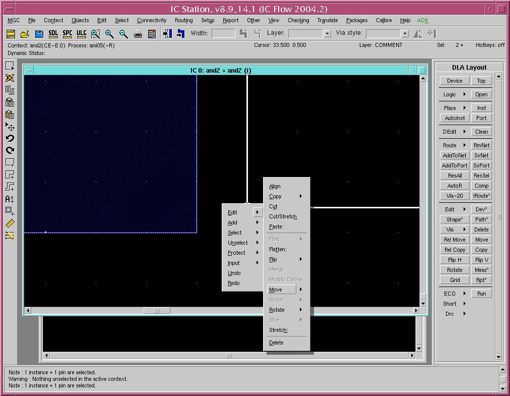
below. Select the second nor2 cell (draw a box that includes
part of it) then right click the mouse and select edit->move
as shown.
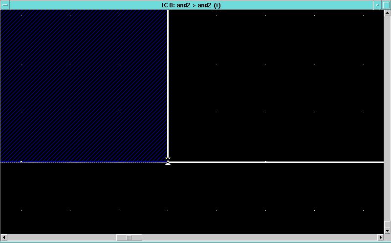
2.8 You will see the move dialogue box open in the bottom
corner of the screen as shown below:

2.9 Left click on the "+" labeled From.
Now move the mouse and left click on the lower left corner of the selected
nor2
cell. This establishes your working reference point on the nor2
cell
you wish to move. Now left click on the lower right corner of the
unselected nor2 cell. The two nor2 cells should now
be perfectly abutted and your IC layout window should now look like:
2.10 Press F2 to unselect the middle nor2 cell.
Zoom out then zoom in and repeat the procedure to mate the rightmost nor2
with the left and middle cells. Unselect again, zoom all and your
IC layout window should look as below:
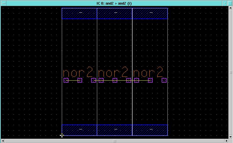
2.11 Now all the VDD and GND connections are made and the relevant
overflows are gone.
3. Wire the hierarchical and2 gate.
Now we will wire the connections within the and2 gate
to match the schematic. You could do this manually using paths and shapes
as you've done before. If you opt for this route, remember that there is
a Metal1 blockage over all of the nor2 gates, so all routing
over the cells at this level must be Metal2 or higher. Also remember
that there are rules against stacking vias!
Hint: While routing and autorouting you will
need to select individual overflows. It is sometimes hard to do this
on the IC layout window. But you can make the schematic window active,
select the wire you wish to route in that window then make the IC layout
window active and the appropriate overflow should be selected. This
is an important benefit of connectivity editing...
In order to illustrate its use, the ICStation
auto router will be used to route the interconnections here.
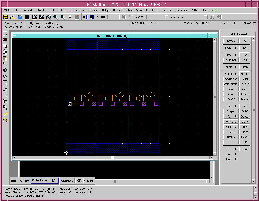
3.1 Press F2 to unselect everything. Select the overflow
between the left most two ports on the leftmost nor2 gate. In the
DLA
Layout palette, click on the AutoR button. When the
prompt bar appears at the bottom of the screen, the Probe Extent
item will be highlighted. The autorouter is asking you to specify
the area in the layout within which it can route the selected net. You
specify this by drawing a box around the area where you would like the
wire to go with the left mouse button. Do that now by drawing a box
around the two ports where the selected overflow is connected as shown
below. Magically, a METAL2 wire will appear between the ports and
the overflow will disappear.
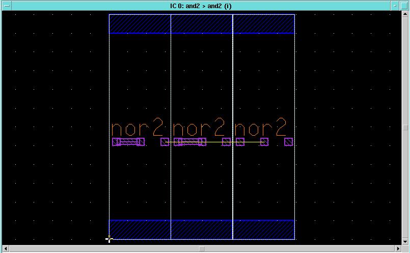
3.2 Select the overflow between the middle nor2 gate's inputs
(it may be easier to select it on the schematic) and autoroute that as
well. Now your layout should look like:
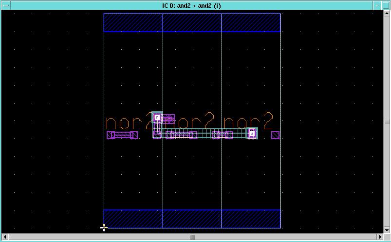
3.3 Select the connections between the output of the left nor2s
and the inputs of the right nor2 (this may be easier in the schematic as
well) and autoroute them. You'll have to give the autorouter a larger
area to work with, so draw the Probe Extent box larger in the Y direction
this time. If one or both of the routes does not get done, you probably
didn't draw the box big enough, so try again. The end result will
be something like this:
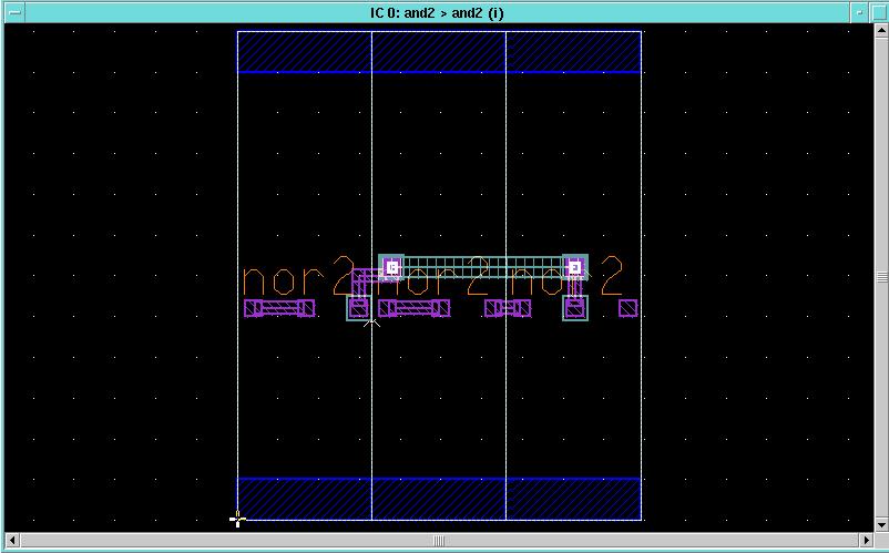
3.4 Do a DRC check at this time to see if the autorouting was
done OK. If you end up with a routing like the one above, you will
get errors because VIA2 between METAL2 and METAL3 was placed above a VIA
between METAL1 and METAL2 by the autorouter. This was most likely
caused by it not seeing the VIA inside the nor2 cell. There are several
ways to fix this, but the easiest way is to add METAL3 blockages over the
METAL2 ports. This will cause the autorouter to use METAL2 to come out
from over the ports before it uses METAL3 (and the associated VIA2s).
3.5 Make the IC layout window active and type "undo"
in the window then press the Return key. Do this several times
until the overflows you just routed return. Unselect all (F2)
and add a shape of METAL3_BLKG around the remaining unrouted METAL2 ports
at least one lambda outside them. Make sure that the aspect is set
to internal. Select the two unrouted overflows and route them again.
Continue this process until your layout passes DRC. Hopefully, the
result will be something like the one below:
4. Add ports and text
4.1 Now add the three ports from the schematic (in1,
in2 and out1) one at a time. The procedure is the same for each.
a) Press F2 to unselect everything
b) Make the schematic window active and select the port you want
to add
c) Click on the Port button in the Place portion
of the palette
d) Make the IC layout window active
e) Zoom to where the port belongs and place it
Repeat the above procedure for all three ports. Unselect (F2)
then add a METAL1.PORT shape over the VDD rail. Use Object->Make->Port
to make it a port (VDD, POWER, IN). Repeat for the ground rail (GND,
POWER, IN).
4.2 Select Object->Add->Add Text on Ports to add
the port names to the ports.
4.3 Remember from lab5, if you were going to use this and2 cell
as a part of a larger design, you would need to place metal with Aspect=Both
over each of the ports AND you would need to make that metal part of the
port. For instance, the VDD port is on METAL1.PORT. You would
need to add METAL1 with Aspect=Both over the top of the METAL1.PORT and
you would need to use the Connectivity->Port->Add to Port
function to combine the METAL and the METAL1.PORT.
4.4 Now that ports are placed and the cell is completed routed,
run LVS as you did in lab5 to make sure the layout matches the schematic.
Remember that you must close the schematic Logic->Close before you can
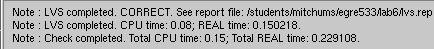
run LVS. If your LVS is successful then the bottom left status
line should look as shown below (LVS completed. CORRECT.).
If not, go back and fix any errors.
4.5 Once you have a successful DRC and LVS, save the cell.
5. Extract a netlist and do post-layout simulation with MachTA
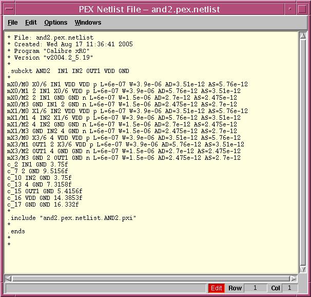
5.1 Use Calibre->Run PEX to extract the
parasitics as you did in lab5. The resulting spice file should look
as shown below. (Don't worry about checking it line by line - just
make sure it looks similar.)
5.2 Exit IC Station then use the Unix command window to
fix the and2.sp file for simulation with MachTA:
>> cell_sim_prep and2
5.3 Start MachTA on
the fixed and2 Spice file:
>> mta -ezw -t $ADK/technology/mta/ami05
-tc TYP and2.sp &
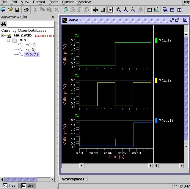
5.4 Plot v(in1), v(in2), and v(out1), force some values on
the in1 and in2 signals and run the simulation. You should
see a result like this - its still an AND gate!
5.5 Close the EZ wave viewer and exit MachTA.