Post-Layout Simulation with ADiT and EZWave
1. Extract the Spice representation of your inverter
In this lab, you will use ICStation/Calibre
to extract a Spice representation of the inverter you drew in the previous
tutorial. Then you will use the ADiT simulator to simulate the Spice representation.
1.1 Move into the directory you created for lab2. Then
start
ICStation:
>> cd egre533/lab2
>> adk_ic &
1.2 In ICStation,
use the Cell Open item in the Session palette to open the my_inv
cell you previously created. From the top menu bar select Calibre->Run
PEX to start a Parasitic EXtraction. Calibre PEX is a separate
program which will extract information about the connectivity and associated
capacitances and resistances in your layout. You will need to fill
in a few screens to properly initialize Calibre PEX. The Calibre
PEX setup information will be saved, however, so you only need to enter
it once. The Calibre PEX extraction tool reads in your layout from
a GDS-II (Graphic Design System II) file and creates a Spice netlist file
suitable for simulation.
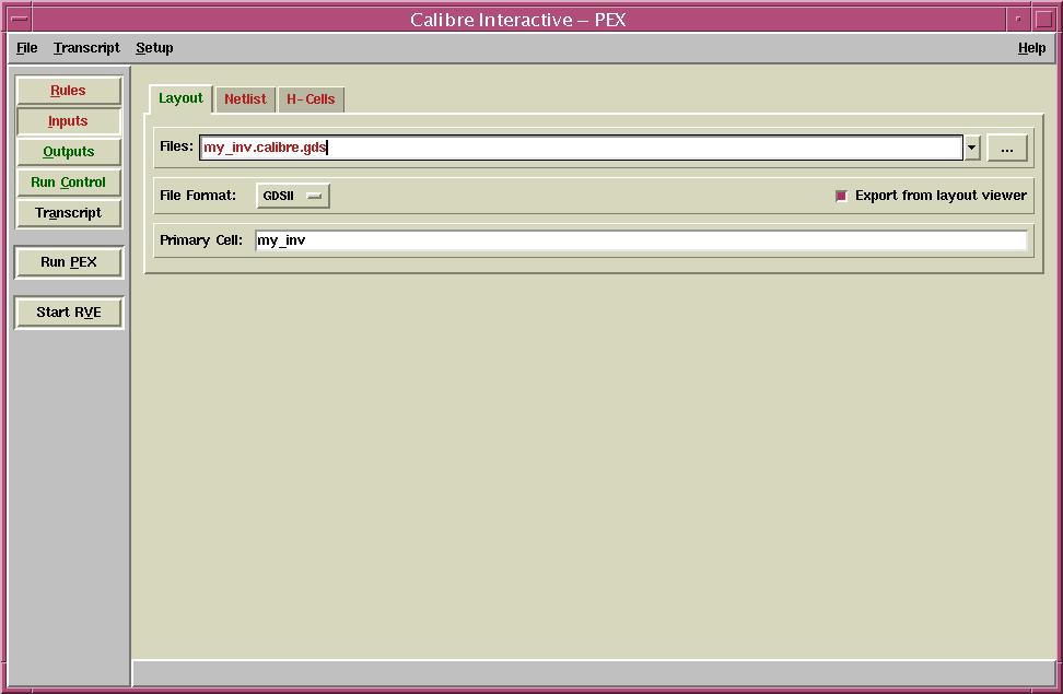
1.3 The first screen displayed by Calibre PEX is the Inputs
screen, as shown. Don't make any changes. The Layout
tab specifies the input file (my_inv.calibre.gds), the file format
and primary cell. Notice the Export from layout viewer
button is checked. This instructs Caliber PEX to use the layout viewer
to create a new copy of the GDS file before extraction. If you uncheck
this box then you must use the IC Station Translate menu item to
create a GDS file for Calibre PEX. The Netlist tab
specifies a source netlist, meaningless for this exercise but useful for
other layout extractions. The H-Cells tab specifies
a Hierarchical Cell source file, again meaningless for this exercise.
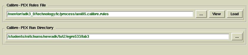
1.4 Left click once on the Rules button. You must
specify where to find the process rules and layer definitions for Calibre
PEX. Left click once on the ellipsis (three dots) to navigate to
the appropriate rules file. Navigate to the /mentor/adk3_0/technology/ic/process
directory and choose the file "ami05.calibre.rules" as shown:
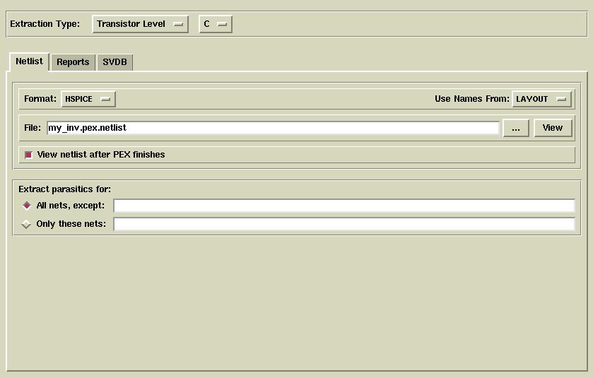
1.5 Left click once on the Outputs button to setup the
output files. Make sure the Extraction Type is Transistor
Level and C. This instructs Calibre PEX to
extract only lumped capacitances at the transistor (or mask) level.
Leave the filename as it is (my_inv.pex.netlist). In
the Netlist tab, make sure the Format is HSPICE
and change the Use Names From: to LAYOUT. Leave
the View netlist after PEX finishes button selected. Do not
change anything under the Reports or SVDB tabs - these are
unimportant for this exercise. Your Outputs setup should look
like:
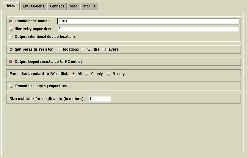
1.6 Select Setup->PEX Options from the top menu bar.
Make sure the button beside Ground node name is selected and type
in GND for the name of the ground node. The Netlist
tab dialogue box should look like:
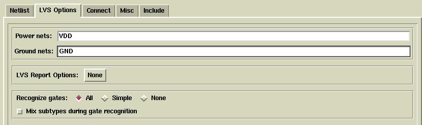
1.7 Now select the LVS Options tab. Enter the names
for the Power nets: and Ground nets: and make sure Recognize
gates: is set to All. The LVS Options dialogue
box should look like:
1.8 Now setup is complete. Left click once on the Run
PEX button to start the extraction. As each stage completes,
information will scroll through the transcript window. If your extraction
is successful a new window will open displaying the spice netlist created
by Calibre PEX. If you do not get a netlist (this make take
a minute or so) then review the transcript window to locate problems and
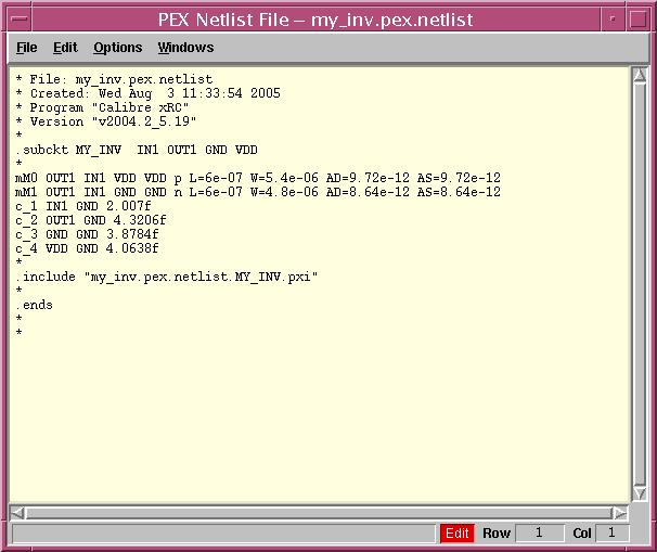
fix them. Your netlist should look similar to:
1.9 Close the netlist window. Close Calibre PEX and
enter runset for the file name when asked to save your runset.
Exit ICStation.
2. "Fix" the Spice file so that it can be simulated with ADiT
ADiT is another version of a Spice simulator that is much faster than
Accusim. Unlike Accusim, it does not operate on a schematic, but
on a text input file in Spice format like the one you just generated from
ICStation
using Calibre PEX. However, the Spice file you just generated
is not quite complete and needs to be "fixed" before you can simulate it
with ADiT.
2.1 Notice the netlist file from Calibre PEX contains a subcircuit
called MY_INV that consists of two transistors mM0 and mM1
(the ones you created) and several capacitors c_1 .. c_4 (parasitics).
In order to simulate this circuit, we need to get rid of the subcircuit
notation, add voltage sources for VDD and GND, and add model statments
for the transistors.
2.2 From the command line, run the cell_sim_prep_vasim
script on the my_inv Spice file:
>> cell_sim_prep_vasim my_inv
This will generate a file called my_inv.sp which is correct
for simulation with ADiT.
2.3 Open the resulting my_inv.sp file. You will see a file
like the one below:
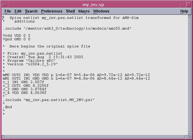
Notice that there are two new voltage sources added for VDD and GND, model
statments for the devices added, and the subcircuit line has been removed.
This file is ready to simulate with ADiT.
2.5 You will notice that the cell_sim_prep_vasim script also
created a file called my_inv.cir Use the text edit to open this
file as well. It should look like the one below:
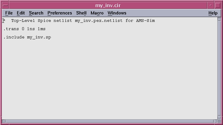
This file specifies the type of analysis that should be run by the ADiT
simulator - in this case, a transient, or timing analysis. The 1ns parameter
is the minimum time step for the simulation and the 1 ms is the maximum
time that the simulation can run. If, in simulating larger cells, you need
to simulate for longer than 1ms, you will need to edit this file to change
this parameter.
2.6 Close the text editor.
2. Simulate the my_inv Spice description with ADiT
2.1 The ADiT simulator is accessed through a GUI interface that is
very similar to the one used for the ModelSim VHDL simulator. This GUI
is called vasim.
First, you must create a work library for vasim:
Start vasim:
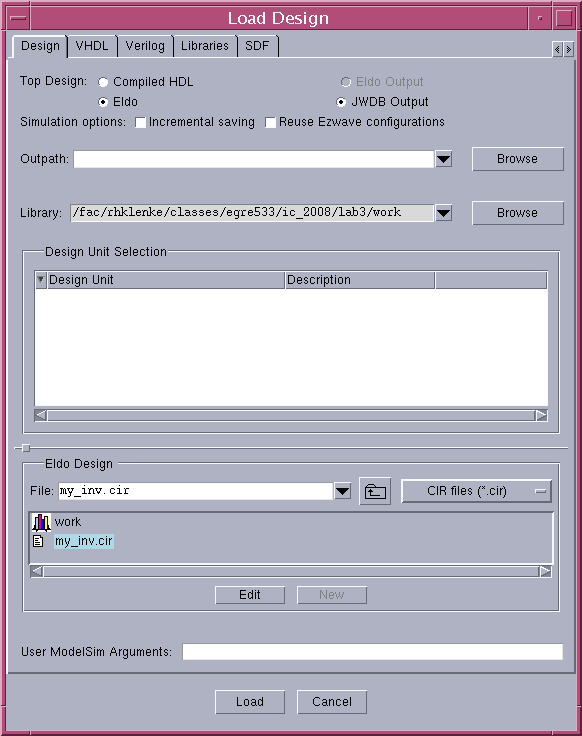
You should see the Load Design window open up. Fill out the
window fields so that it looks like the one below and click Load:
2.2 Loading the design will take a few moments. When "Load done" appears
in the transcript of the main vasim window, select the View->Debug
Windows->All Windows menu item to bring up all of the simulator
windows. The result should be a set of windows as shown below:
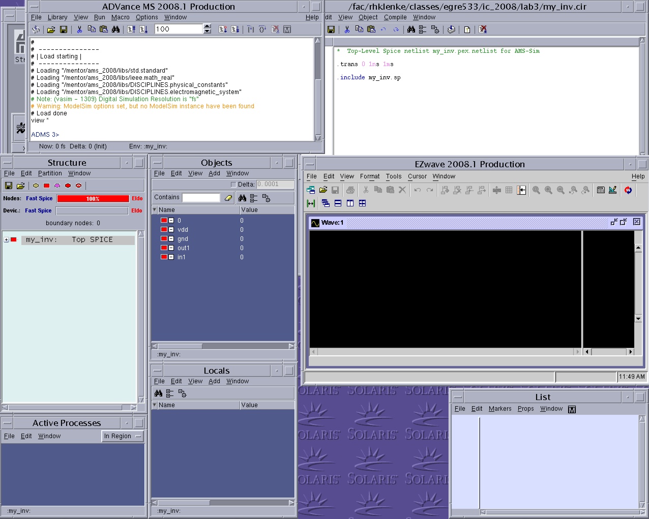
2.3 Notice in the Structure window, you can see the my_inv
component and that the simulator is set to Eldo. Eldo is the normal Spice
simulator (also used by Accusim) and it is fine for small components. However,
for larger components, you will want to use the ADiT simulator. To do so,
make sure that my_inv is highlighted in the Structure window and use the
menu item Partition->Simlator->ADiT in that window to change
the simulator to ADiT.
2.4 In order to simulate a Spice cell in vasim,
you have to force values on its inputs - just as you did for the transistor
level schematic in Accusim. There are several ways to do this in vasim,
but one of the best ways is to create a "do file." for the component. A
"do file" is simply a list of simulation commands. In this case, we need
commands to trace signals we want to look at, commands to force values
onto input signals, and run commands to run the simulator.
Use the text editor to create a "do file" called my_inv.do, that
looks like the one below:
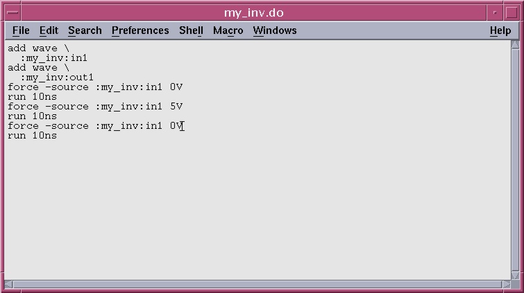
The commands in this file add the IN1 and OUT1 signals to the wave window
(so we can see what is happening on them), forces the IN1 input to 0 volts,
runs the simulation for 10 ns, forces IN1 to 5 volts, runs the simulation
for 10 ns more, forces IN1 back to 0 volts, and runs the simulation for
a final 10 ns.
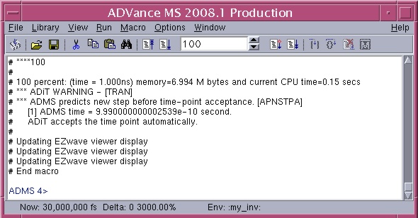
2.5 To "run" the do file, simply type the following command in the vasim
transcript window:
You will see messages from the ADiT simulator appear in the transcript
window as it is running. At the end, the vasim
transcript window should look like this:
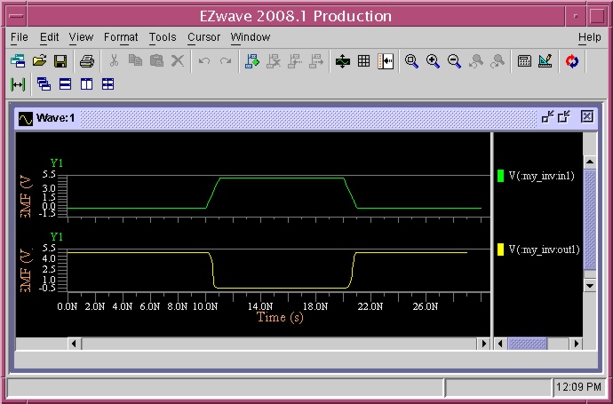
Once the simulation is complete, the IN1 and OUT1 waveforms should appear
in the EZwave window:
2.6 Exit vasim by typing
"quit" in the vasim transcript window.