Full Custom Design of an Inverter using IC Station and the AMI Rules
INTRODUCTION
In this tutorial you will learn how to use Mentor Graphics ICStation
to construct a mask level layout of an inverter. You will manually create
the artwork which specifies transistor layouts and their interconnection.
This process is somewhat tedious but will help you understand IC layout
- how you make and connect transistors to form an integrated circuit.
Later tutorials teach automated ways and faster methods. You will also
verify that there are no design rule errors in the final layout. You will
translate a static CMOS inverter onto an NWELL and PWELL process using
AMI's 0.5 micron technology.
Important Shortcut Keys for IC Station:
-
Ctl-K: Toggle between absolute and relative screen coordinates
on the screen
-
F2: Unselect everything. Use frequently to avoid accidentally
moving or deleting selected items
-
Esc: Terminate the current operation. Use to quit adding
shapes or paths
-
Shft-F8: Zoom to fit window
-
Numeric Pad +: Zoom in
-
Numeric Pad -: Zoom out
-
PageUp: Move window up (object down)
-
PageDown: Move window down (object up)
-
Ctl-PageUp: Move window left (object right)
-
Ctl-PageDown: Move window right (object left)
-
Left-Mouse Button: Select, draw or access top pull-down menu
or side palette items
-
Right-Mouse Button: Open local popup menus
1. Start IC Station and Open a new cell
1.1 Create a directory for this lab and move into it. Open
IC Station:
>> cd egre533
>> mkdir lab2
>> cd lab2
>> adk_ic &
1.2 In the session palette window, click on CREATE with LMB (left
mouse button). In the Create Cell dialog box that comes up, set
the cell name to my_inv, the cell type to block, and select
No connectivity as shown. Click on the Browse button beside
the Process item and navigate to the $ADK/technology/ic/process/ami05
process file and click OK. Click on the Browse button beside
the Rules File item and select the ami05.rules file and click
OK.
The resulting dialog box should look like the one below:
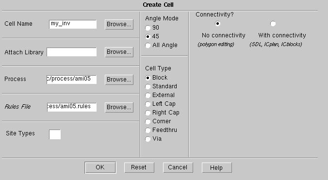
Click the OK button in the Create Cell dialog box and new window
should open with the message Cell "/students/.../egre533/lab2/my_inv"
reserved for edit. Note that in ICStation,
before you can edit a cell, it MUST be reserved for edit. If you close
a cell and reopen it, or save a cell, it is no longer reserved for edit.
You must use the File->Cell->Reserve
menu item to reserve the cell for edit after it has been closed or saved.
2. Layout polygons for the transistors of the inverter
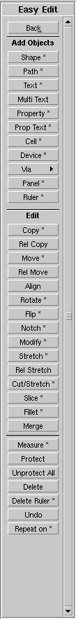
2.1 You will need to draw, modify polygons etc., so click (LMB) on
Easy
Edit in the IC Palette. It will change to that shown on the right.
To create an n-channel device we need POLY over ndiff
. Here are the drawing steps you will be performing for reference.
Detailed instructions for drawing follow this reference list.
Steps to make an inverter:
(a) Construct an ACTIVE polygon.
(b) Surround the ACTIVE with N_PLUS_SELECT. The intersection
of the two gives ndiff.
(c) Create a POLY over ndiff and extends beyond the active
area. This results in the gate.
(d) Surround the whole thing with P_WELL.
For a p-channel MOSFET, we need an N_WELL as well. The steps
are as follows:
(a) Construct an ACTIVE polygon.
(b) Surround the ACTIVE with P_PLUS_SELECT. The intersection
of the two gives pdiff.
(c) Create a POLY over ndiff and extends beyond the active area.
This results in the gate.
(d) Surround the whole structure with N_WELL.
Before you start, notice that at the top of the ICStation
window, under the menus, is another bar with the word Cursor: in
it followed by two numbers. These numbers are the current position of the
cursor in lambda coordinates. They are relative to an origin that is fixed
in the window where you will draw your inverter. The coordinates given
below for drawing the inverter refer to these numbers. NOTE: when you place
the cursor in the window and click to start editing, the cursor will sometimes
place a mark in the drawing (a large cross) and the label at the top of
the window will change to To Mark: . In this case, the numbers now
refer to the coordinates relative to the mark placed in the drawing. You
can hit
<Control K> on the key board to switch the numbers back
to absolute coordinates.
2.2 Click on Shape* under Add Objects in the palette window
with LMB. Click on the Options in the prompt bar which appears at
the bottom left hand corner. Choose N_PLUS_SELECT and leave Aspect
set
to internal.
2.3 Hit <Control K> to change back from To Mark: to
Cursor:
and press the LMB at -2,-9 and drag it to 16,11 and release. Use the Zoom->
Out... menu item twice to zoom out. Use the popup menu for Edit->
Copy and place the copy at -2, 34. Press F2 to unselect all.
Be sure to click Cancel in the prompt bar (or press the Esc
key) to get rid of it after you are finished with that particular operation!
2.4 Use the pop-up menu, Select-> Edge, choose the top edge of
the top rectangle. Click on the Rel Move item in the Easy Edit
palette . In the prompt bar enter the following (use tab key).
X Offset = 0; Y Offset = 2 & click OK. The top edge should
move up by 2 units.
2.5 We need a PMOS and an NMOS, hence we need to change the top shape's
layer from N_PLUS_SELECT to P_PLUS_SELECT.
2.6 Select the top N_PLUS_SELECT, use the pull-down menu Object->Change->Layer,
select
P_Plus_Select, click OK.
2.7 Now we will add the N_WELL. Select the P_PLUS_SELECT, use
the pulldown menu: Edit->Resize.
In the dialog box enter, (use the tab key).
Resize by =4; select Shapes/paths are copied and resized;
and
set From Layer=P_PLUS_SELECT; To Layer= N_WELL then hit enter. A
green rectangle representing N_WELL will appear.
2.8 Unselect all (F2) then select the N_PLUS_SELECT layer. Add
a P_WELL 4 units away as you did above for the N_WELL.
2.9 You have laid the ground work, let us make the transistors. From
the palette menu, Add->Shape , choose ACTIVE and draw a rectangle
from 0,-7 to 14, 9 and from 0,36 to 14,54.
2.10 Now add the gate Click on Path (Under Add Objects), click
on Options, choose POLY and enter 2 for width in the dialog
box that comes up. (Aspect=Internal, Padding=NoPadding, PathStyle=Center
and Endstyle=Normal.) Place the cursor at 7,56 and single click with
the LMB, go all the way to 7,-9 and double click. Hit F2 to unselect
all.
2.11 Hit Shift F8 to view all. Draw a counter clockwise
circle with the MMB (middle mouse button) around the lower set of rectangles
to zoom in. Choose
Add->Shape, click on options and choose CONTACT_TO_ACTIVE.
Draw a 2x2 rectangle at location 2,-4.
2.12 Click with the LMB inside the contact and hit Rel Copy
in the palette, or use the pull-down menu, Edit->Copy->Relative,
in
the prompt bar enter:
Number = 1; X Offset = 0; Y Offset = 8, hit return.
2.12 Using this mechanism, or simply by selecting the contact and hitting
Copy
and placing the copy manually, place a copy of the contacts at locations
2,50 2,44 2,38 10,50 10,44 10,38 10,-4 and 10,4. Hit F8 to view all and
unselect all by drawing a U with MMB.
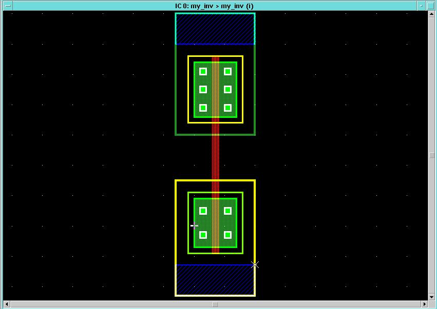
2.13 Power rails for VDD and GND (+5V and ground) must be visible both
internally and externally so other circuit components can be attached.
To add power rails, choose METAL1, set Aspect to Both
and draw a rectangle (a shape) starting at -6,-23 and ending at 20,-13.
Hit F2 to unselect all and Esc to stop adding shapes.
2.14 Use Select->Area
to select the METAL1 and copy it at -6,60. Unselect all.
2.15 Use Select->Edge
to move the top edge of the N_WELL to y = 70. Hit F2. Use
Select->Edge
again to move the bottom edge of the P_WELL to y = -23. Hit F2.
Your
layout should look like the one shown below.
2.16 Let us do quick DRC (Design Rule Check) check of the structure
that we have completed so far. The DRC will tell you if you have
any shapes too close together or any partial connections. In the Easy
Edit palette, click on Back. In the
IC Palettes palette,
click on ICrules. In the ensuing ICrules palette, click on
Check. Click OK in the prompt bar. You should get a
total of 12 errors. (The error count is in the lower left hand
portion of the main adk_ic window.)

2.17 Under Set Scan to in the ICrules palette, click on
First. At the bottom of your screen, it will come back with a message,
"[Current DRC] Result 1 of 10 in RuleCheck bad_contact_active: Contact
to active must consist of active, CONTACT_TO_ACTIVE, and METAL1". At
the same time, the specific contact in the window will flash.
Click on Next to see the next error. Continue clicking
on Next, and you will see errors for all of the contacts. Finally,
you will get two errors for contact in the P_WELL and N_WELL
" [Current DRC] Result 1 of 1 in RuleCheck bad_nwell: Nwell must
have well contact"
"[Current DRC] Result 1 of 1 in RuleCheck bad_psubstrate: Psubstrate
must have a substrate contact"
These errors will be fixed in the next section.
Note that it is good to perform frequent DRC checks
during the design of your circuits. That way, you avoid having to make
extensive changes as a result of not having enough room to move things
around to eliminate a design rule violation!
THE LAYOUT OF THE TRANSISTORS IS COMPLETE, YOU NOW NEED TO "WIRE" IT.
3. Wire the devices to form the inverter
3.1 Go back to the Easy Edit palette. Choose Add->Path,
select METAL1 (Aspect = Internal) with a width of
4 and connect the top left contacts to VDD (3,37 --> 3,60) and the
bottom left contacts to GND (3,7 --> 3,-13). Also connect the right
set of contacts together with METAL1, width 4 (11,-5 --> 11,53).
You will need to use <Control K>.
3.2 Use the pop-up menu and Select->All.
Use the pull-down menu, Edit->Flatten.
Click OK in the prompt bar. This will change all the selected paths
into shapes. (Shapes are sometimes easier to deal with because you can
select and move one of their edges at a time).
4. Add input and output port connections for the inverter
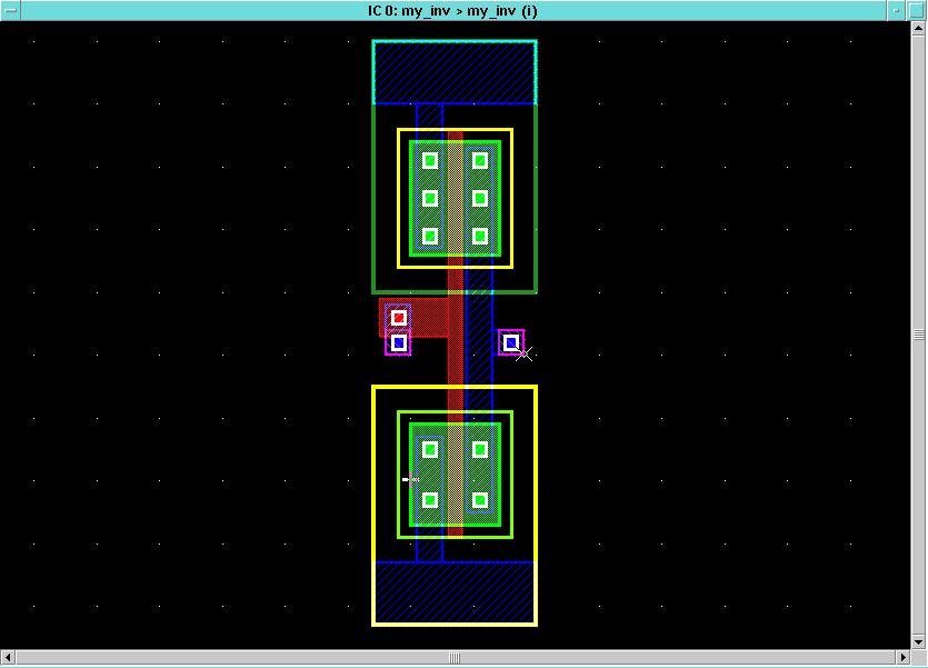
4.1 Zoom in around the area between the two transistors using O middle
mouse button stroke or + key. You will now build up the input
and output ports. The input port must come up the following layers:
POLY, METAL1 and METAL2 (it also needs CONTACT_TO_POLY to go from
POLY to METAL1 and VIA to go from METAL1 to METAL2). The output
port need only go from METAL1 to METAL2 (it also needs VIA to go between
METAL1 and METAL2). The POLY, CONTACT_TO_POLY, METAL1 and VIA shapes
need only be visible internally. But the METAL2 shape will connect
to other devices and so must have Aspect=Both.
4.2 Use, Add->Shape,
choose POLY and create a shape from -5,23 --> 6,29. Add a 2x2 CONTACT_TO_POLY
at -3, 25 to connect METAL1 and POLY.
4.3 Use, Add->Shape,
choose METAL1 from the tiny palette, make a rectangle from -4,28
--> 0,20 and 13,24 --> 18,20.
4.4 Add a 2x2 VIA at -3,21 and 15,21 to connect metal one to
metal two.
4.5. Use, Add->Shape,
choose METAL2 with Aspect=Both from the tiny palette,
make a rectangle from -4,20 --> 0,24 and 14,20 --> 18,24. Your layout
should now look like this:
5. Create ports for place and route
Since this cell is to be used in a much larger circuit, it needs to
have points where the connections can be made, i.e. input, output, VDD,
GND. This connectivity information is specified by using separate
layers. For example, the top METAL1 rectangle will become the physical
connection to VDD. The topmost METAL1 shape calls out the location
for the metal inside the integrated circuit. You must add a METAL1.PORT
shape over the top of the METAL1 shape to hold the connectivity (port)
information. The same is true of the GND connection at the bottom
of the layout and of the in1 and out1 connections on the gate and source/drain
METAL2 connections.
The port structure must be correct in order for the auto placement and
autoroute tools to be able to work correctly. The correct structure
for a port is:
1) METALx with Aspect Both to make physical connections
2) METALx.PORT with Aspect Both to recognize connectivity information
3) Text on the METALx.PORT shapes required by the parasitic
extraction tool (PEX)
For each port (VDD, GND, in1, out1) you will:
-
Add a METALx.PORT shape where x=1 for VDD,GND and x=2 for in1,out1 (these
.PORT shapes must have Aspect=Both)
-
Use the Objects->Make->Port menu item to define the new shape
as a port
Then after all the ".PORT" layers are added, you will use the Objects->Add->Add
Text On Ports menu item to bind the port names to the ports.
Finally, after the text has been added to the .PORT shapes, you will
use the Connectivity->Port->Add to Port menu item to add
the METALx shapes to the port.
5.1 Press F2 to deselect everything. Start with the
input port, the gates to the transistors. In the Easy Edit menu,
select the Shape button then choose METAL2.PORT and make
sure to set Aspect=Both. (You set Aspect to Both so
that your ports are visible internally to the inverter and externally to
other modules.) Add the METAL2.PORT shape from -4,20 to 0,24.
Then press the Esc key once to end adding shapes but leave the METAL2.PORT
selected. From the top menu bar choose Objects->Make->Port.
In the dialog box enter the following:
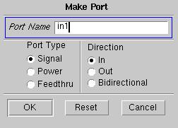
Port Name = in1; Port Type = Signal and Direction
= In then click on OK.
5.2 Press F2 to deselect everything again. Then place
a METAL2.PORT with Aspect=Both from 14,20 to
18,24. Again press the Esc key to stop adding shapes.
Again choose the Objects->Make->Port menu item. Now you are
making an output port so this time fill in:
Port Name = out1; Port Type = Signal and Direction
= Out then click on OK.
5.3 Again press F2 to deselect. Then place a METAL1.PORT
shape with Aspect=Both from -6,60 to 20,70. Again press
the Esc key then choose Objects->Make->Port,enter the following
and click on OK.
Port Name = VDD; Port Type = Power and Direction =
In
5.4 Again press F2, place a METAL1.PORT shape with
Aspect=Both
from -6,-23 to 20,-13. Press the Esc key then choose Objects->Make->Port,
enter the following then click
OK.
Port Name = GND; Port Type = Power and Direction =
In
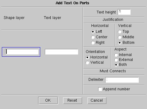
5.5 Now from the top menu select Objects->Add->Add Text On
Ports. Click OK on the popup dialogue box (if you leave
the layers blank IC Station will assume you mean all the METALx.PORT layers).
You will get a message saying "4 text object(s) added" and you should
see the names appear over the ports. Press F2 to unselect everything.
5.6 Now for the tricky part. You must select a METALx.PORT layer,
select the corresponding METALx layer and use Connectivity->Port->Add
to Port to add the METALx to the port. Here is the fool-proof
way:
a) Press F2 to unselect everything.
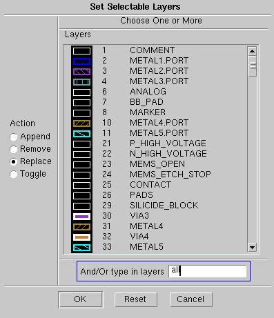
b) Use the top menu item Others->Layers->Set Selectable Layers
to set the selectable layers to METAL1.PORT. Now only METAL1.PORT shapes
can be selected.
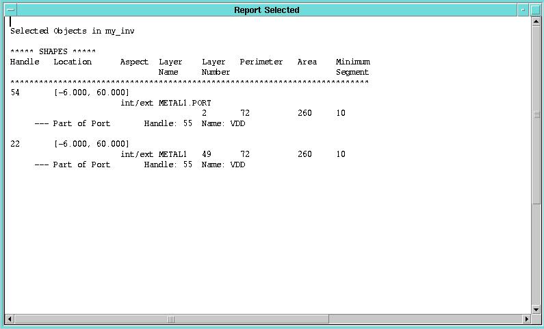
c) Select the top METAL1.PORT (VDD) shape by left clicking on it.
Status line should say Shape ... layer 2 (METAL1.PORT) ... area is 260
... perimeter is 72 ... part of port "VDD"
d) Use Others->Layers->Set Selectable Layers to set the
selectable layers to METAL1.
e) Select the top METAL1 shape by left clicking on it. Status
line should say 2 shapes are selected.
f) Select the Connectivity->Port->Add to Port item from
the top menu.
g) Select the Report->Selected menu item from the top
menu and verify the report looks as shown below.
h) Close the report window, press F2 to unselect and repeat
steps (a) through (g) for GND, in1 and out1. Remember in1 and out1
are on METAL2...
5.7 Select the Others->Layers->Set Selectable Layers
menu item and type in "all" as shown then click OK
to make all layers selectable again.
6. Create metal blockages for place and route and floorplan shapes
When a cell is used in a bigger circuit then cell to cell interconnects
are routed in metal layers. Since only the ports are visible at this
higher level, a short could be created by the interconnect metal.
To prevent this we need to use blockages. A layer of METAL1.BLKG must be
placed over the entire device to keep metal 1 from being routed across
it. The Aspect option must be set to Both so the blocking
and floor plan layers can be seen at the next higher level.
6.1 Add the following shapes at location -6,70 --> 20,-23. With Aspect
= Both, METAL1.BLKG and fp1.
6.2 To see what is visible to the outside world of this cell. View->Show->Aspect
with Aspect = External. You should see the inverter as below:
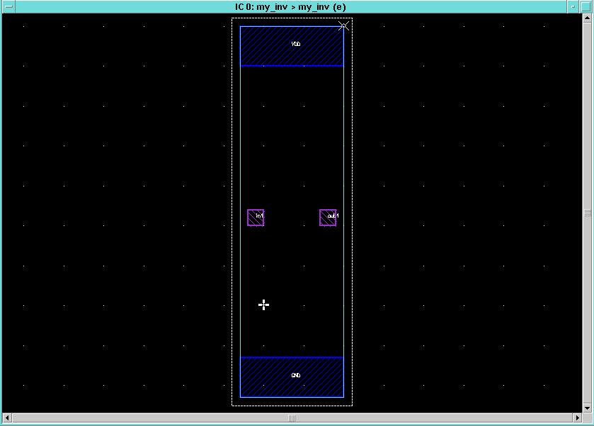
6.3 To see all the layers again, View->Show->Aspect,
Aspect= Both, click OK.
6.4 Save the cell using the File->Cell->Save
Cell menu item.
7. Perform a DRC check and fix the remaining errors
7.1 Click on BACK in the palette and choose IC Rules,
then click on Check. Under Rules File, click on OK.
7.2 You should get two errors. Go to Set Scan and click on
First
to see the first error. Then click on Next to see the next error.
You should the following two messages.
" [Current DRC] Result 1 of 1 in RuleCheck bad_nwell: Nwell must
have well contact"
"[Current DRC] Result 1 of 1 in RuleCheck bad_psubstrate: Psubstrate
must have a substrate contact"
These rules remind us that we need well contacts to avoid latchup problem.
See your text for more details. Create the following structures to eliminate
the errors.
(a) With Aspect = Internal, create a 2x2 rectangle of CONTACT_TO_ACTIVE,
a 6x6 ACTIVE around it and a 10x10 rectangle of N_PLUS_SELECT.
Place it in VDD. Note, you may have to move it about a bit to find a place
where it doesn't violate any design rules.
(b) Create a similar structure but use P_PLUS_SELECT instead
of N_PLUS_SELECT and place it in GND. Make sure that DRC
check results in zero errors.
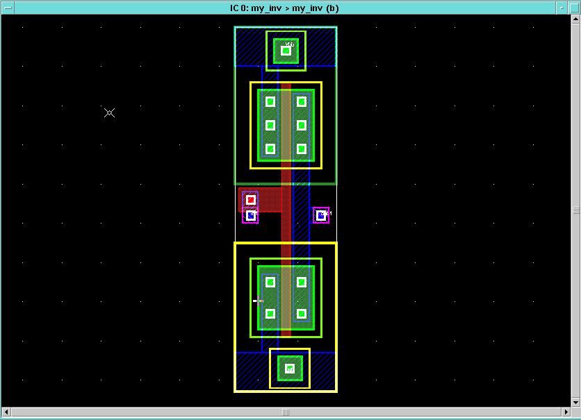
The layout of the inverter is now complete. The final product will look
like the figure below.
7.3 Save the cell and exit ICStation.
Acknowledgment - Based on the tutorial by:
M. Umar Farooq
Department of Electrical Engineering
West Virginia University Institute of Technology
Montgomery, WV 24315
and
Jack Meador
School of Electrical Engineering and Computer Science
Washington State University, Pullman WA 99164