VI. Hierarchical Design Using Pyxis
Table of Contents
Introduction
In this tutorial we will use Pyxis Schematic and Pyxis Layout to create a two input AND gate. We will achieve that by using NOR logic. In previous tutorials we have created a symbol of a transistor level schematic. We will use that symbol to create the AND gate and then we will construct the layout by using the layout created for the corresponding symbol. The final result will be an AND gate created using NOR gates.
Prepare your Workspace
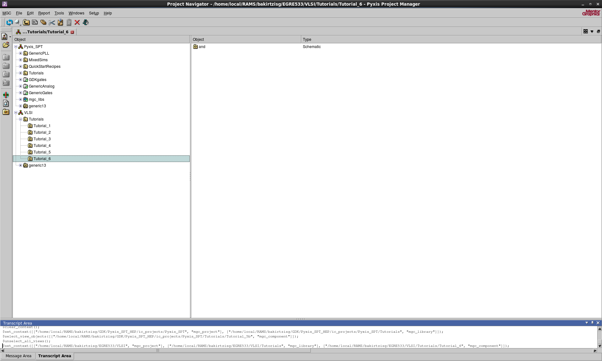
Make a cell named Tutorial_6 in Tutorials and create a schematic named
and.
Creating a Hierarchical Design Using 2 Input NOR Gates
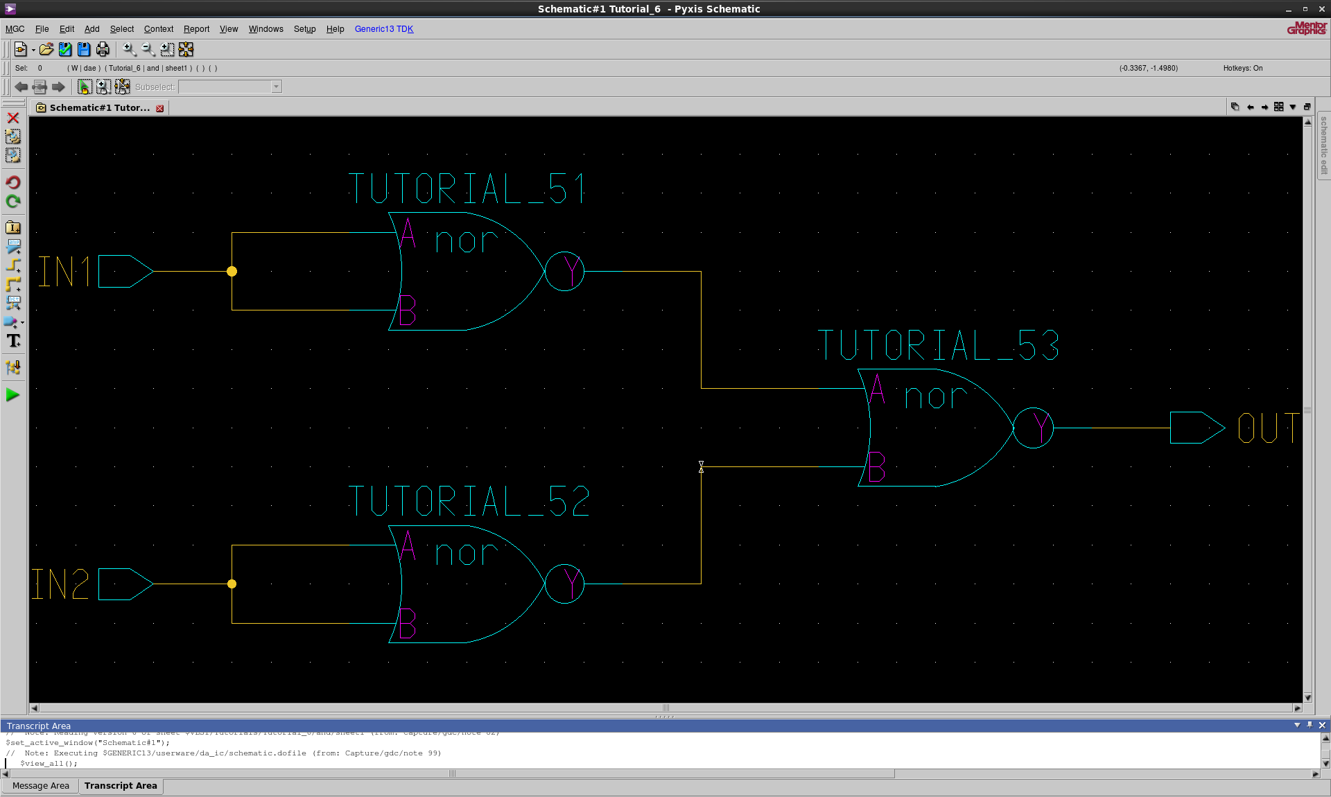
Navigate to Add > Instance... > Choose Symbol and add the NOR symbol
created in Tutorial 5. Use your knowledge of Pyxis Schematic to create an
AND gate using NOR logic as shown below.
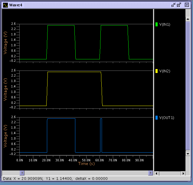
Simulate the resulting schematic as you did in Tutorial 5 to evaluate its
correct operation. Do not forget to put a force on VDD! Note now with two levels of hierarchy some of the
non-ideal effects are showing up. You can see a spike caused by the finite
rise and fall times on the inputs.
Close EZwave and End Sim.
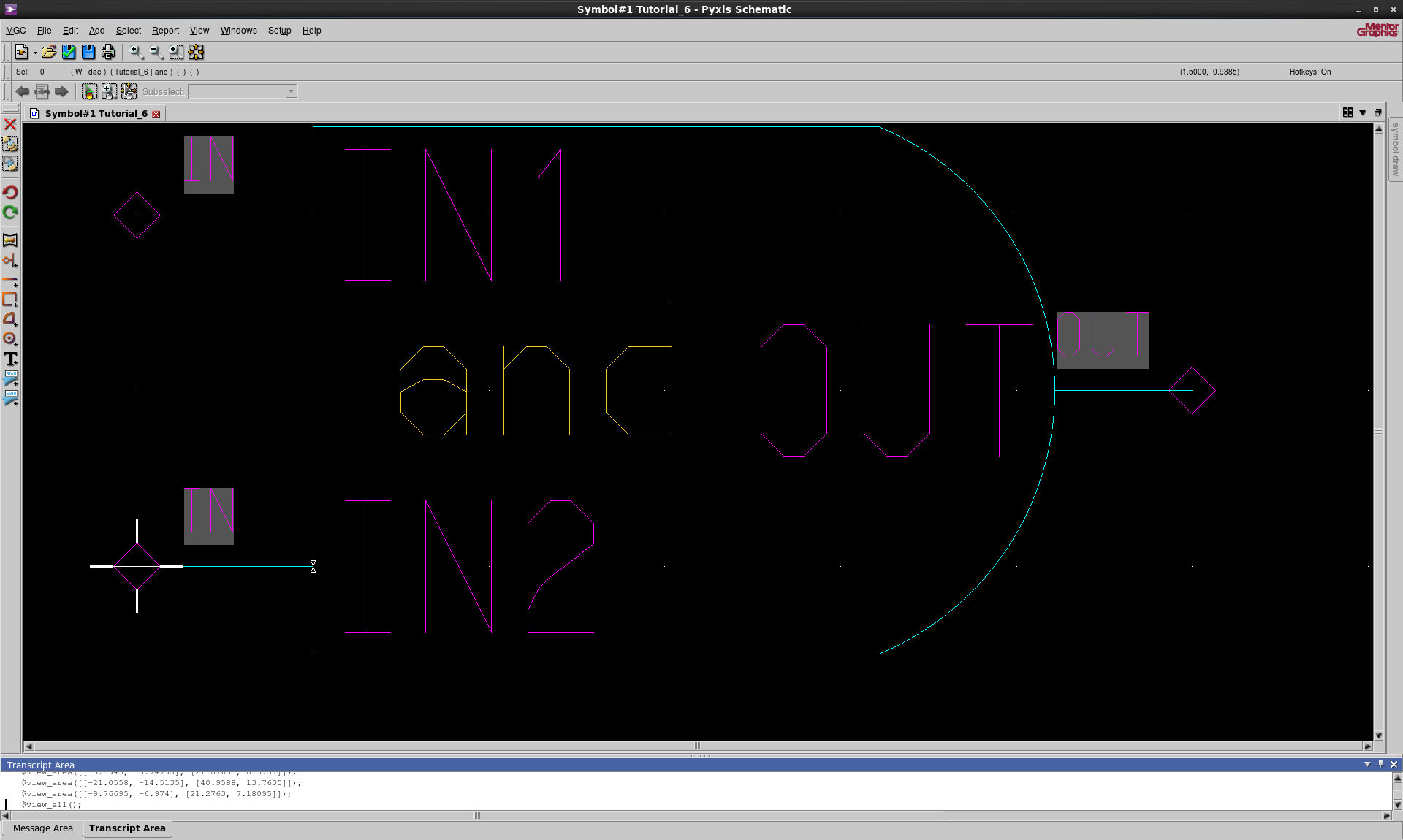
Create a symbol for the AND gate as you did in Tutorial 5 except this
time pick the AND gate shape. Check, save and check the symbol then exit the
symbol editor. Check and save the schematic.
Exit Pyxis Schematic.
Creating the Layout of the AND Gate
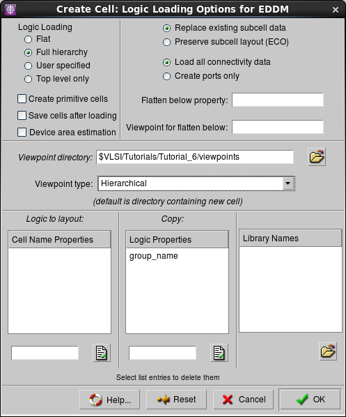
Create a new layout named and in Tutorial_6. In the New Layout
windows choose Logic loading options... and change the viewpoint type to
Hierarchical. Press OK.
At this point the program should have opened your sheet and your empty layout.
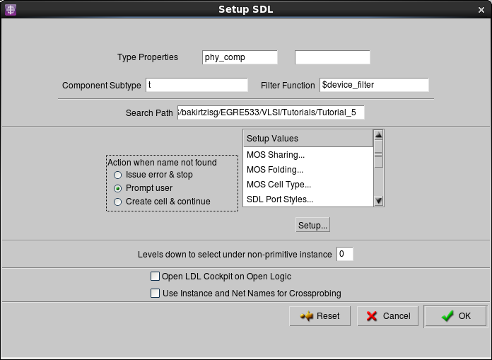
Navigate to Setup SDL and direct the Search Path to
Tutorial_5. This will be different depending on how you have arranged
your folders. A simple way of figuring out the full path is to navigate to
your desired directory in a terminal window using cd and then using the
print working directory command (pwd). You final setup should look like
the one below.
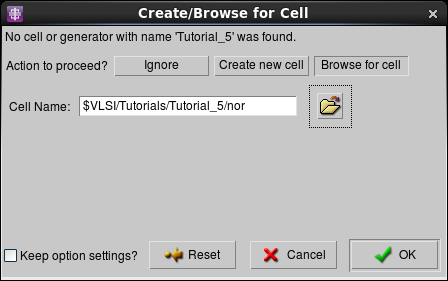
Click on one of the NOR gates and press Add Inst. Because of naming issues the above might not work in generating a layout
automatically. In that case a pop-up window will appear. You just need to
go to Browse Cell and choose your layout schematic for the desired cell.
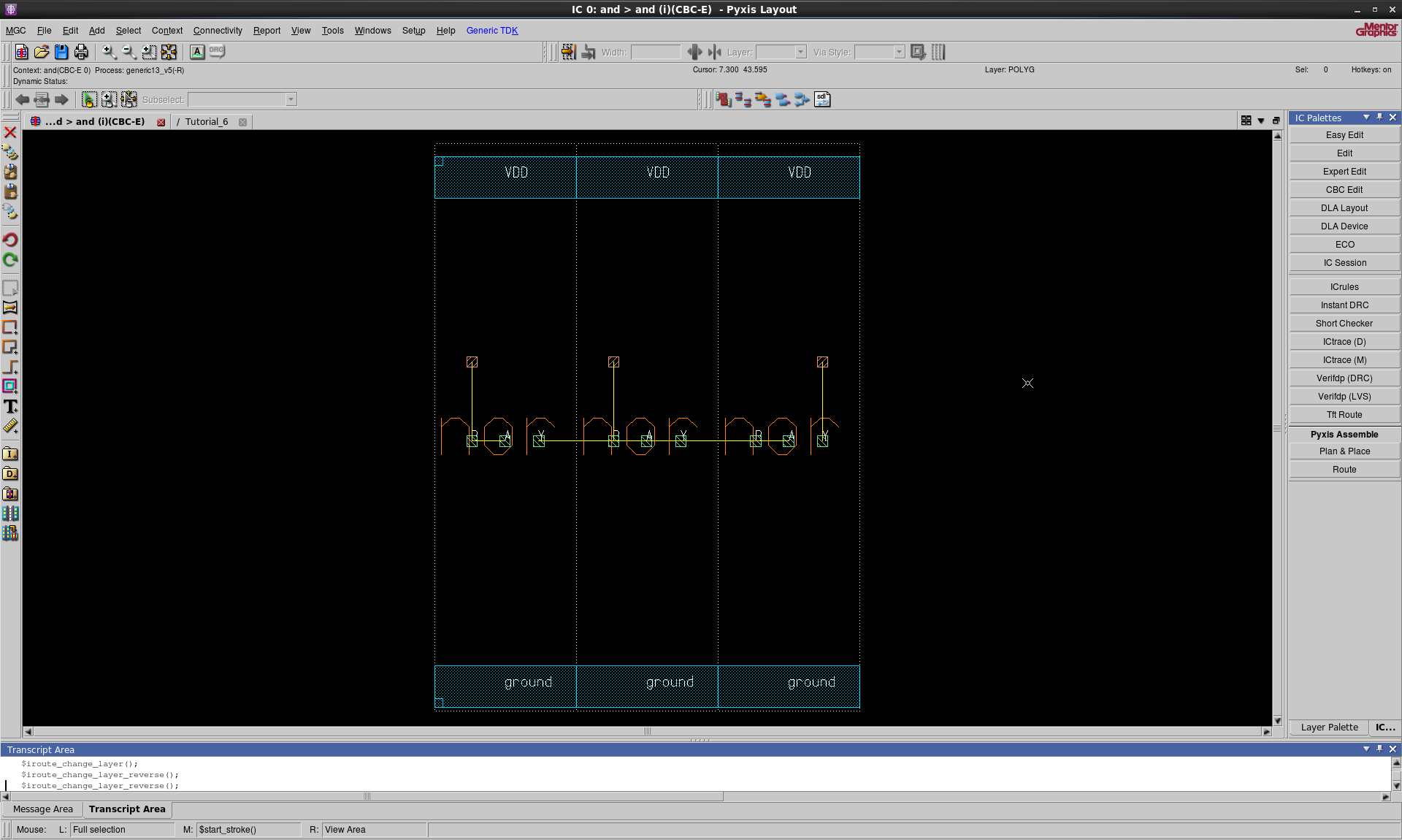
Add all the gates on the layout as shown below. There is an issue when
instantiating an object. You will not see the object itself. Just click on
the sheet and View > All.
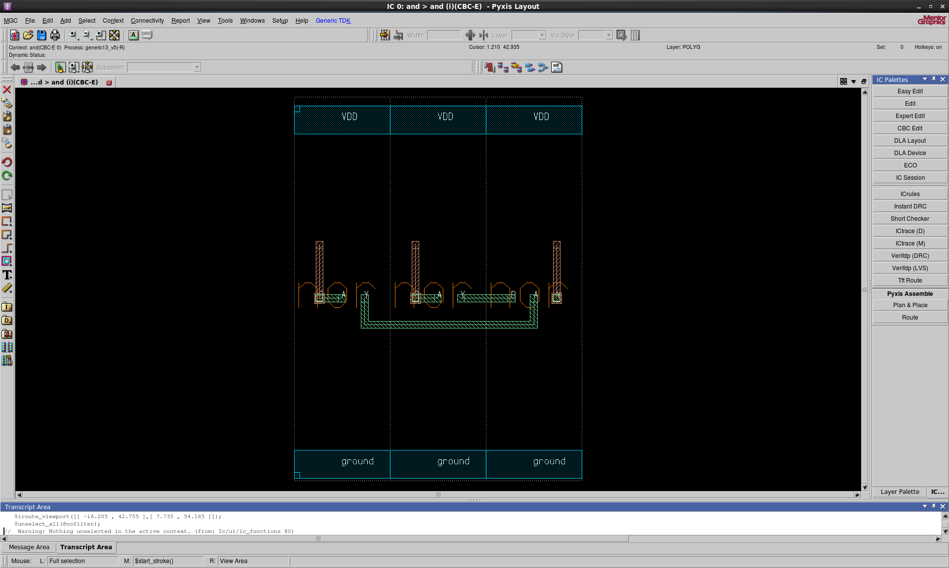
Arrange the gates as shown below. Remember that you can move and align
objects. Simply click on m and then move your object and then click v
to align with another object. If done correctly there should be no
overflows (e.g., yellow lines) between any of the \(V_{DD}\) and ground
rails.

At this point the procedure is the same as before. Add all ports to your
schematic. Because we are going to be wiring between cells it is
recommended that these ports are Metal 3. Since you still need to connect
\(V_{DD}\) and ground to your whole design just click DLA Logic > Port in
your schematic without having anything selected. This will basically
instantiate all ports that haven't been added to your layout but they exist
in the schematic one by one, even the ones that can't be seen in the
schematic like \(V_{DD}\) and ground.
Wire the connections in the circuit correctly as shown below. This step could be different if you've laid your gates differently. Just pay attention to the overflows. You can also choose a net on the schematic and it will be highlighted in your layout.
Finally navigate to Connectivity > Port > Add Text on Ports.... Make sure
the aspect is set to Both.

Run DRC as you've done before. Any errors you get with respect to area of the M3 layer can be ignored as those will be fixed when you interconnect the gate at the next level of hierarchy.
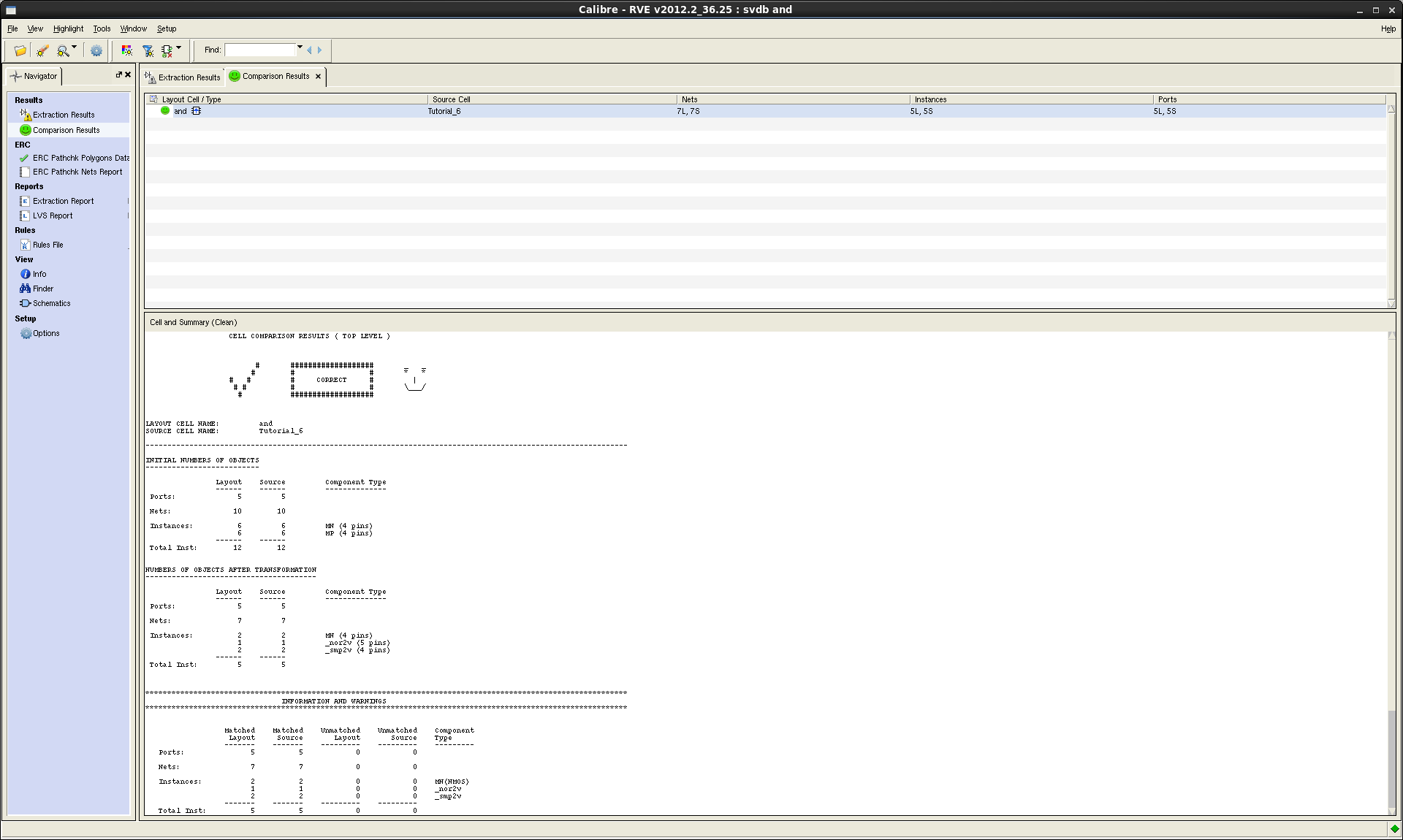
Run LVS. You should get the correct results.
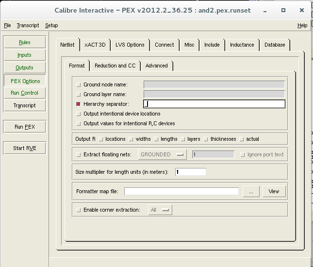
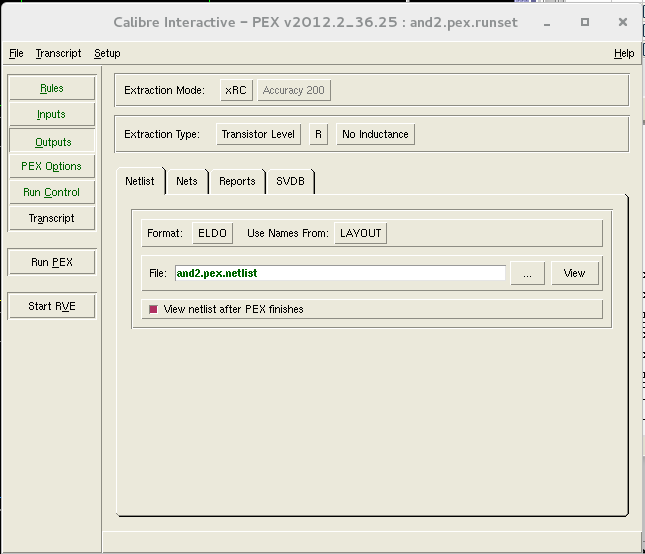
Extract the SPICE file using PEX. You must make one required change in the PEX setup in order for the extracted file to be correct. Under the Netlist tab, select the Hierarchy separator item and change the "/" character to an underscore "_".
Optional: You might also want to set the Extraction Type to R (vs. R + C or the other options). Doing this will tell PEX to only add the parasitic resistances to the netlist and not any of the parasitic capacitances. While this will result in an unrealistic delay model in the simulation, it will allow the signals to transition to the "0" or "1" values much faster (i.e., have very short rise and fall times) which will allow you to verify the correct functionality of your blocks without running the simulation for as long a time.
Simulate the results with VASim as before to ensure the correct operation of your layout.