V. Schematic Driven Cell Layout Using Pyxis
Table of Contents
Introduction
In this tutorial we will use Pyxis Schematic and Pyxis Layout to create a two input CMOS NOR gate. In previous tutorials we have drawn transistors directly from Pyxis Layout. Another way of achieving the same result is to create a schematic and then use Pyxis to automatically construct the shapes necessary that make the circuit.
Prepare your Workspace
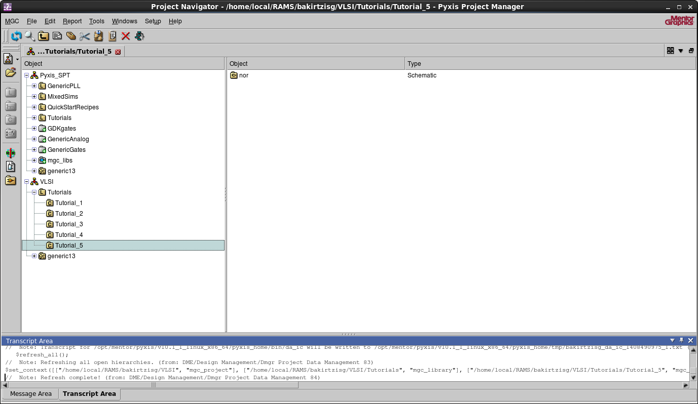
Make a cell named Tutorial_5 in Tutorials and create a schematic named nor.
Creating a CMOS NOR Gate Schematically
Use your knowledge of Pyxis Schematic to create a CMOS NOR gate as shown below.
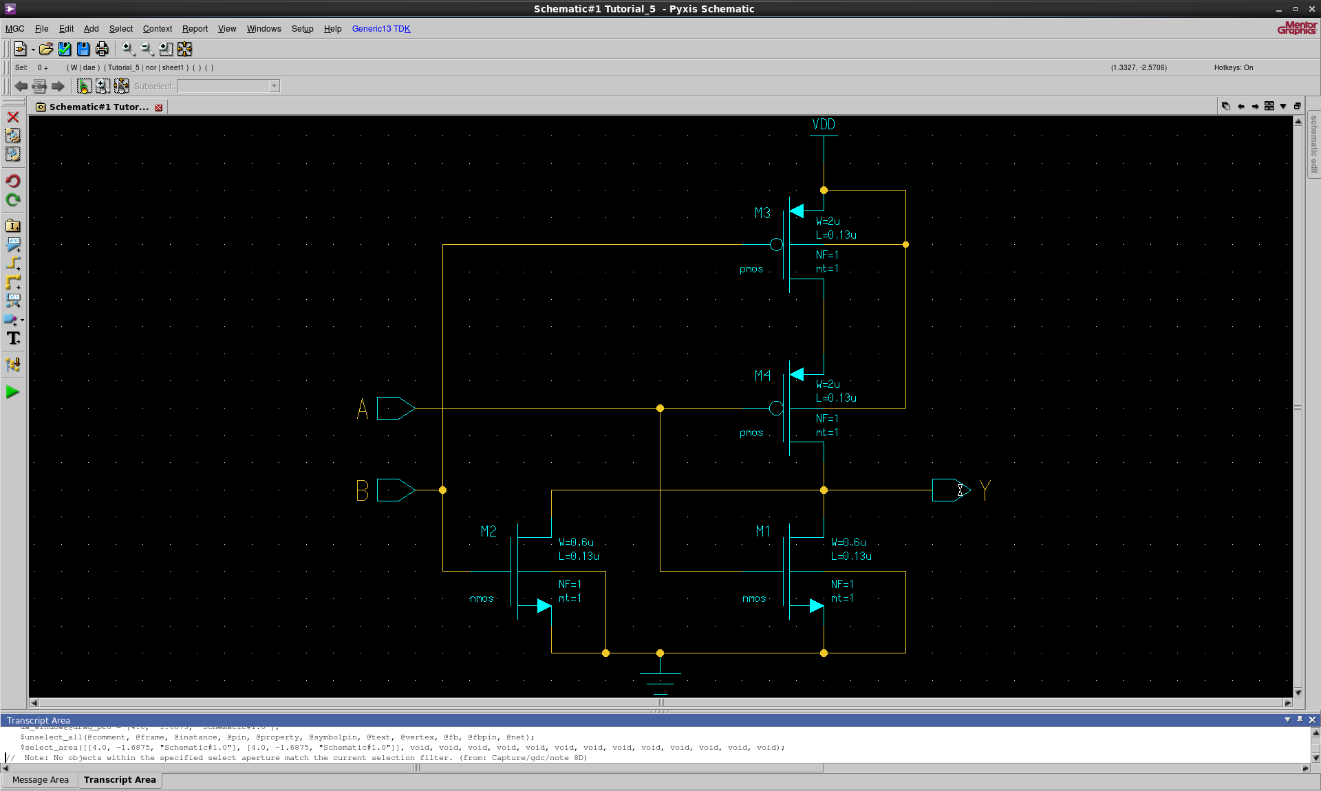
Check your schematic and fix any errors.
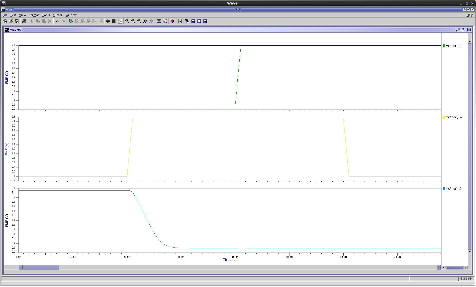
Transient Response of the CMOS NOR Gate
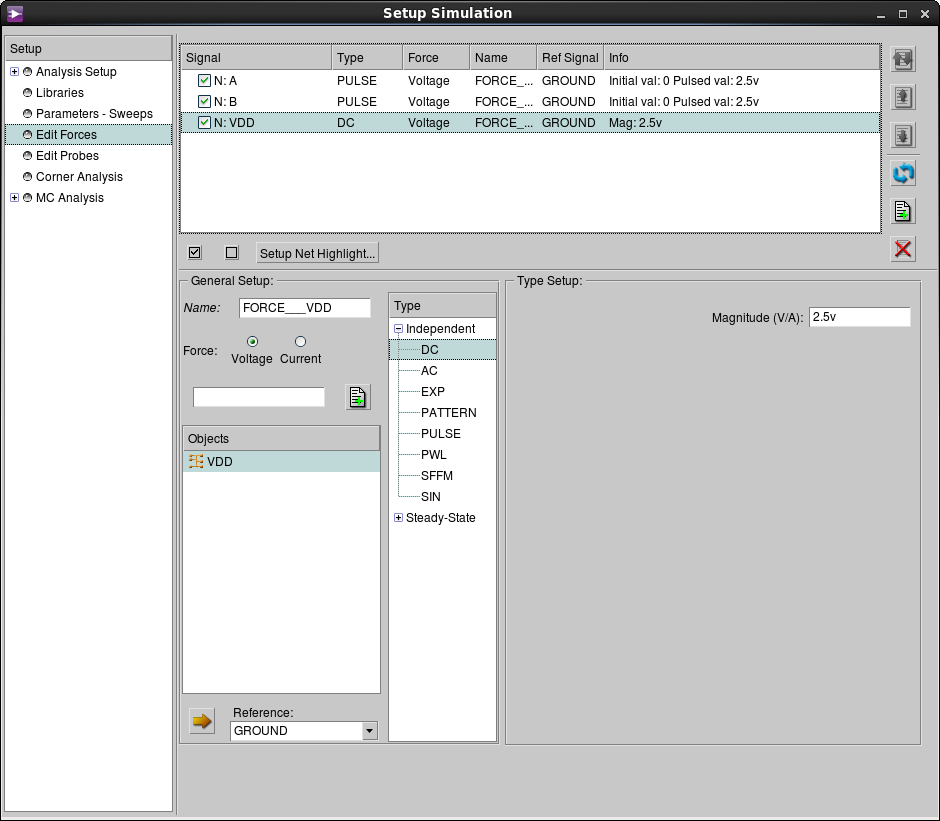
Set the transient analysis as before. Add the necessary forces for the inputs and outputs.
Generate a 100 nanosecond square wave for input 'A'.

Generate a 50 nanosecond square wave for input 'B'.
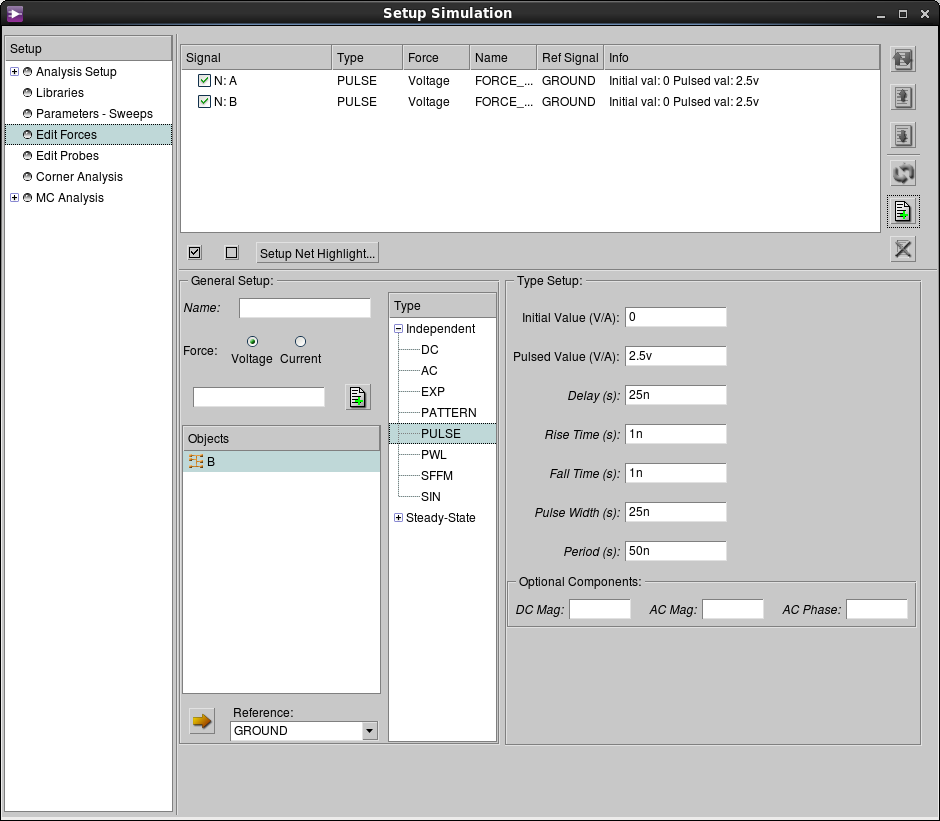
Make the positive supply voltage equal to 2.5 Volts.
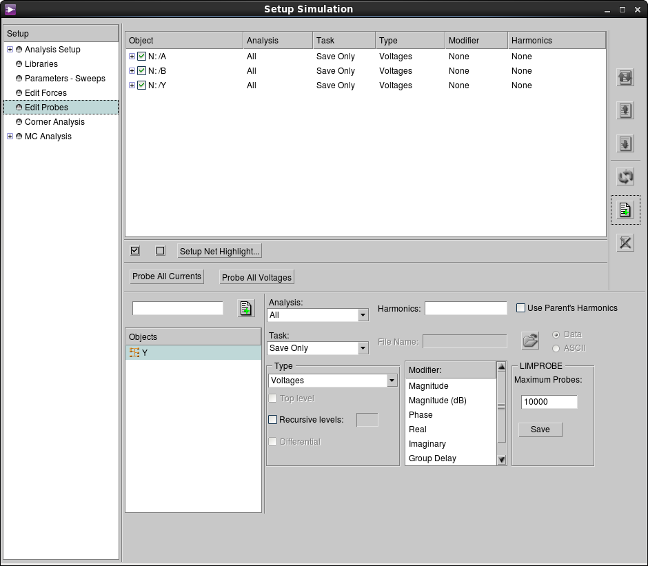
We want to probe inputs A and B and the output Y.
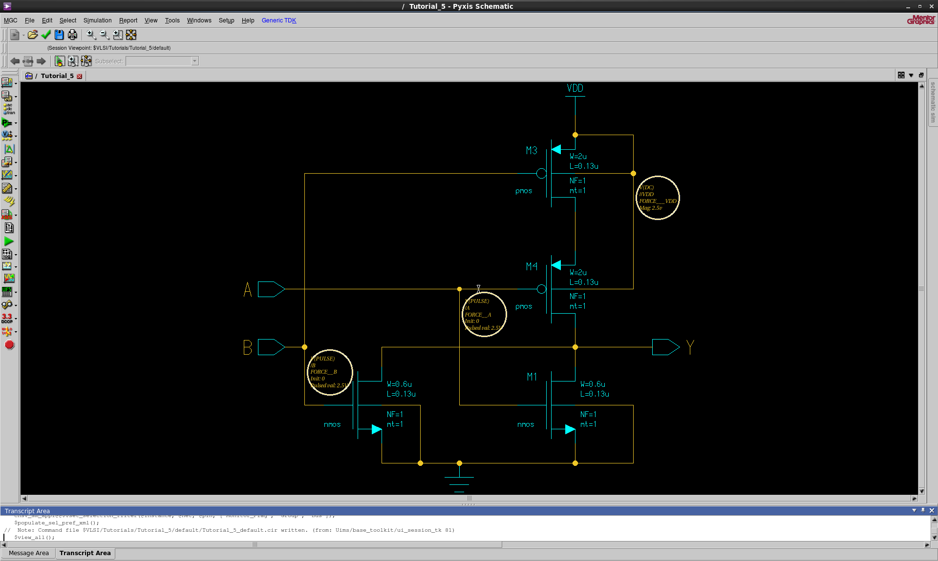
You resulting schematic should look like the one below.
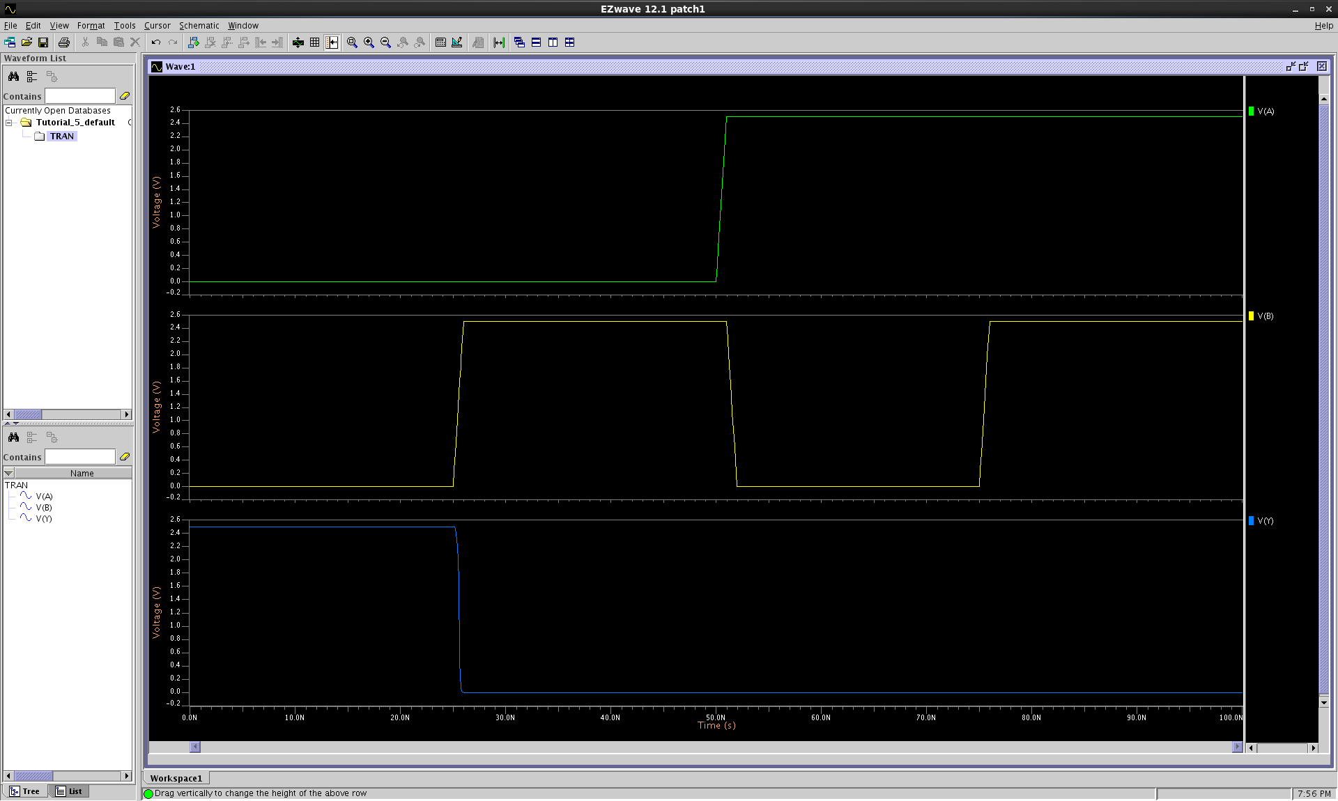
Run the simulation. Evaluate the correctness of your gate. Remember that the equation that governs its operation is expressed as \(Y'=A+B\).
End the simulation.
Creating a Symbol of Your Schematic
There are two reasons we might want to create a symbol for our NOR gate:
- Establish connectivity by defining input and output pins.
- Enable us to use our NOR gate in more complex designs.
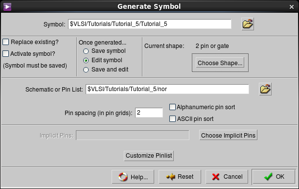
Navigate to Add > Generate Symbol... and left click on Choose
Shape.... Since there is no NOR shape choose the Or gate. Press OK.
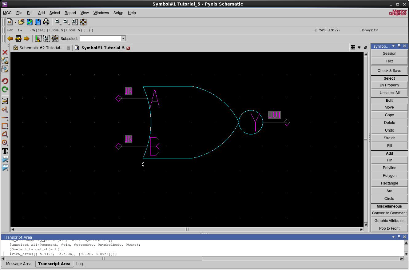
The symbol should automatically have opened in Pyxis Schematic. Select the entire output pin assembly–all three components–by holding down the left mouse and enclosing the pin wire, the text, and the diamond shape. Then move the pin assembly as shown below.
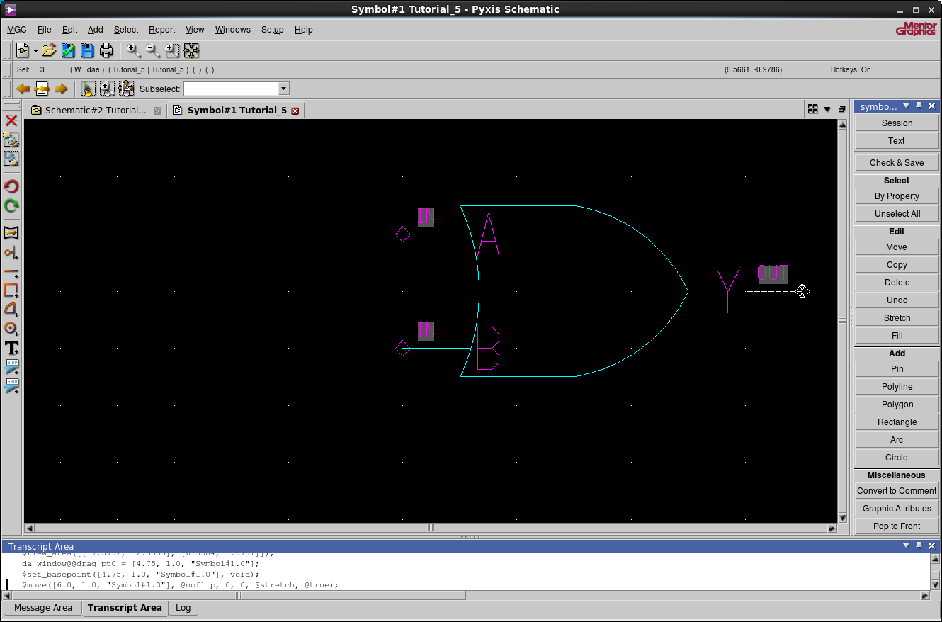
Navigate to Add > Circle and draw a circle between the output and the
rest of the body.
Deselect everything (F2). Check the symbol (File > Check Symbol), then
save (File > Save Symbol) and then check the symbol once again–the
function doesn't actually work the first time. Fix any errors and exit Pyxis Schematic.
At this point we have succesfully created a proper schematic and a proper symbol.
Creating the layout of the CMOS NOR gate Schematically Driven
In Project Navigator under Tutorial_5 create a new layout named
nor. In the next dialog box just press OK.
It is beneficial to combine the two PMOS transistors into a single PMOS
structure. This can be achieved by combining the drain of M2 with the
source of M1.
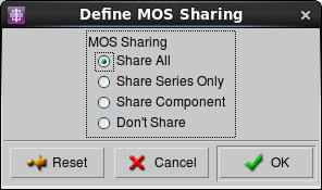
Navigate to Setup > SDL... > MOS Sharing... and click the Setup...
button.
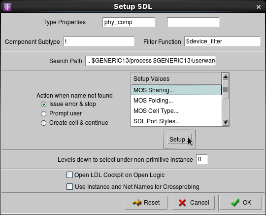
Change the MOS Sharing to Share All and press OK. This will make the program
automatically diffusion share the PMOS and NMOS transistors
correctly. Otherwise you would have to manually merge them (this can be
done either by moving and flipping the transistor into the other one or
choosing the correct nets on each transistor and navigating to DLA Device
> Edit > Join)
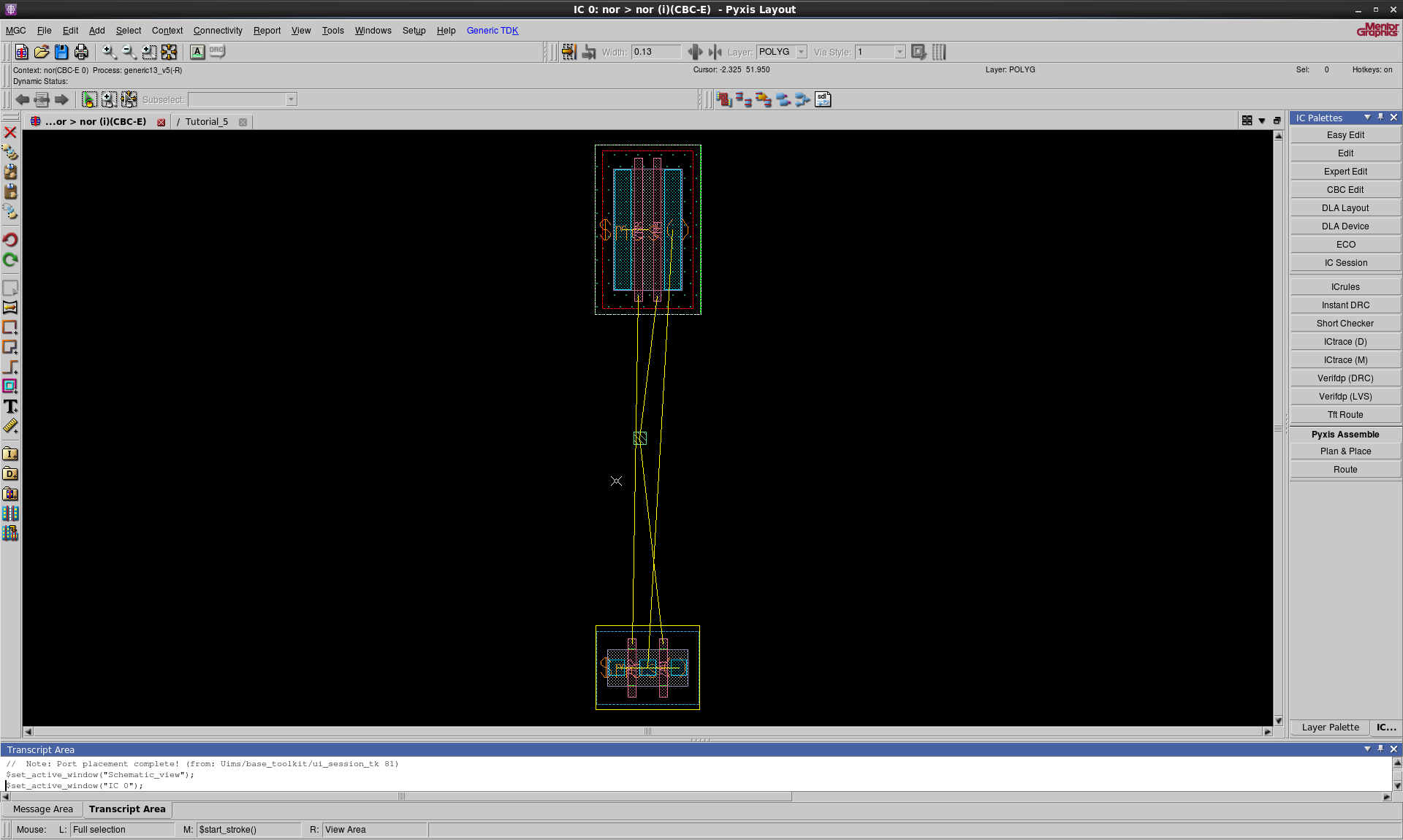
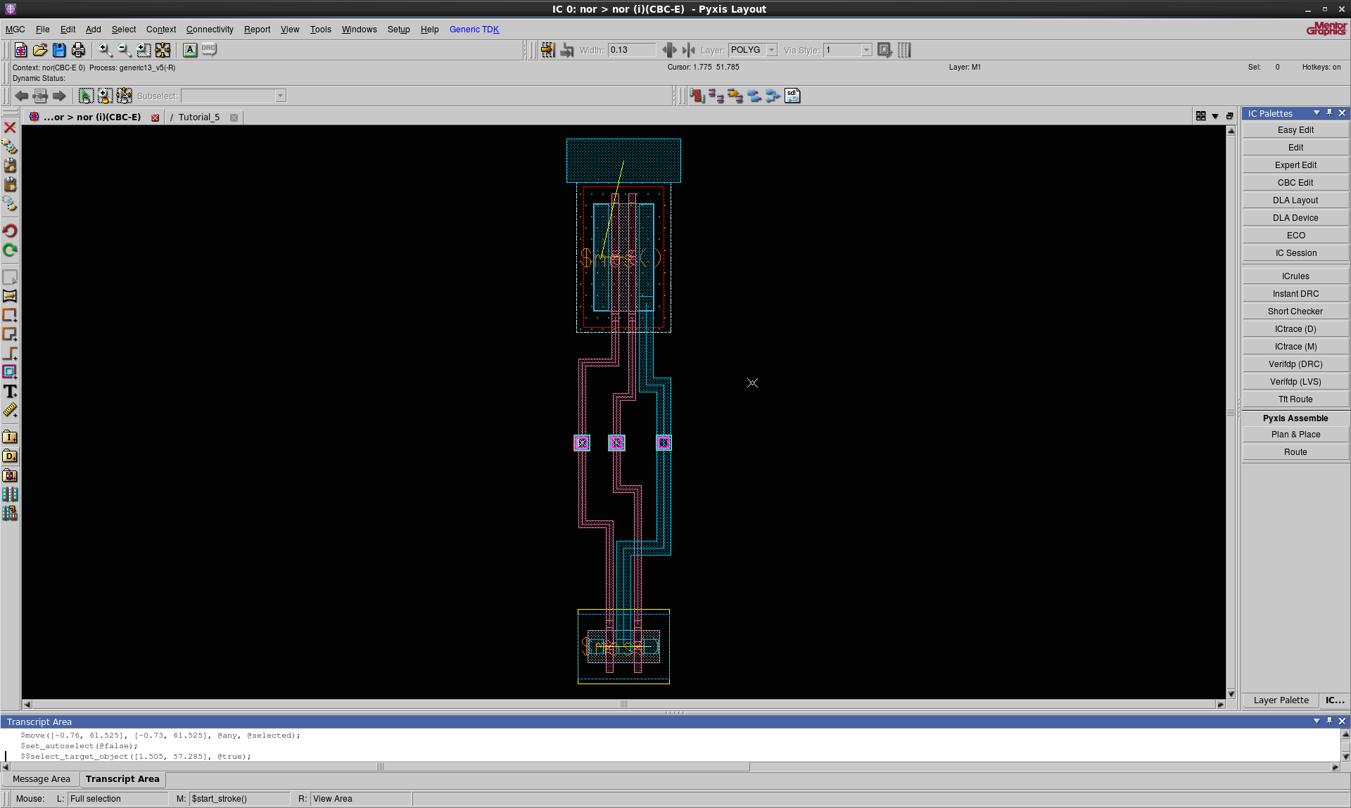
Then, go to your schematic and select DLA Layout > AutoInst. This will
automatically instantiate your transistors. Make sure nothing is selected
when you do that action. The resulting schematic should look like the one
below:

Remark: The yellow lines on the layout mean that there are missing
connections/overflows. Also, you might need to move the transistors closer
together. As with previous tutorials click the transistor shape and press
m then move the transistor and align using v to the middle of the other
transistor in the layout.
In previous tutorials we have used Metal 1 to represent the inputs of the inverter. However, for most practical purposes where the cells are going to be used in hierarchical design, we would want the inputs to be something else. Hence, this time and any subsequent times you should use Metal 2 to represent the input and output ports. \(V_{DD}\) and the reference node should still be Metal 1.
Go back to your schematic and select the input 'A' branch. Then navigate to
DLA
Logic > Port
. Change the input to Metal 2 by going up two levels from POLYG
(you can achieve that by pressing 4 twice). Align it as shown below.
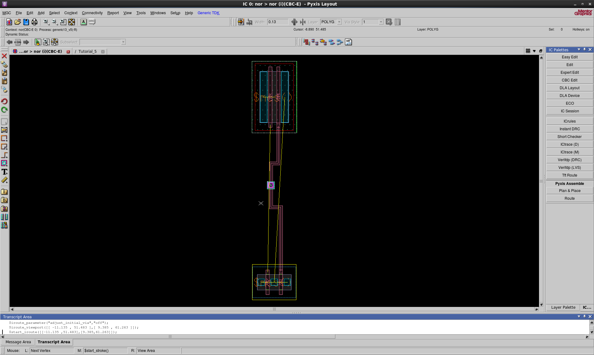
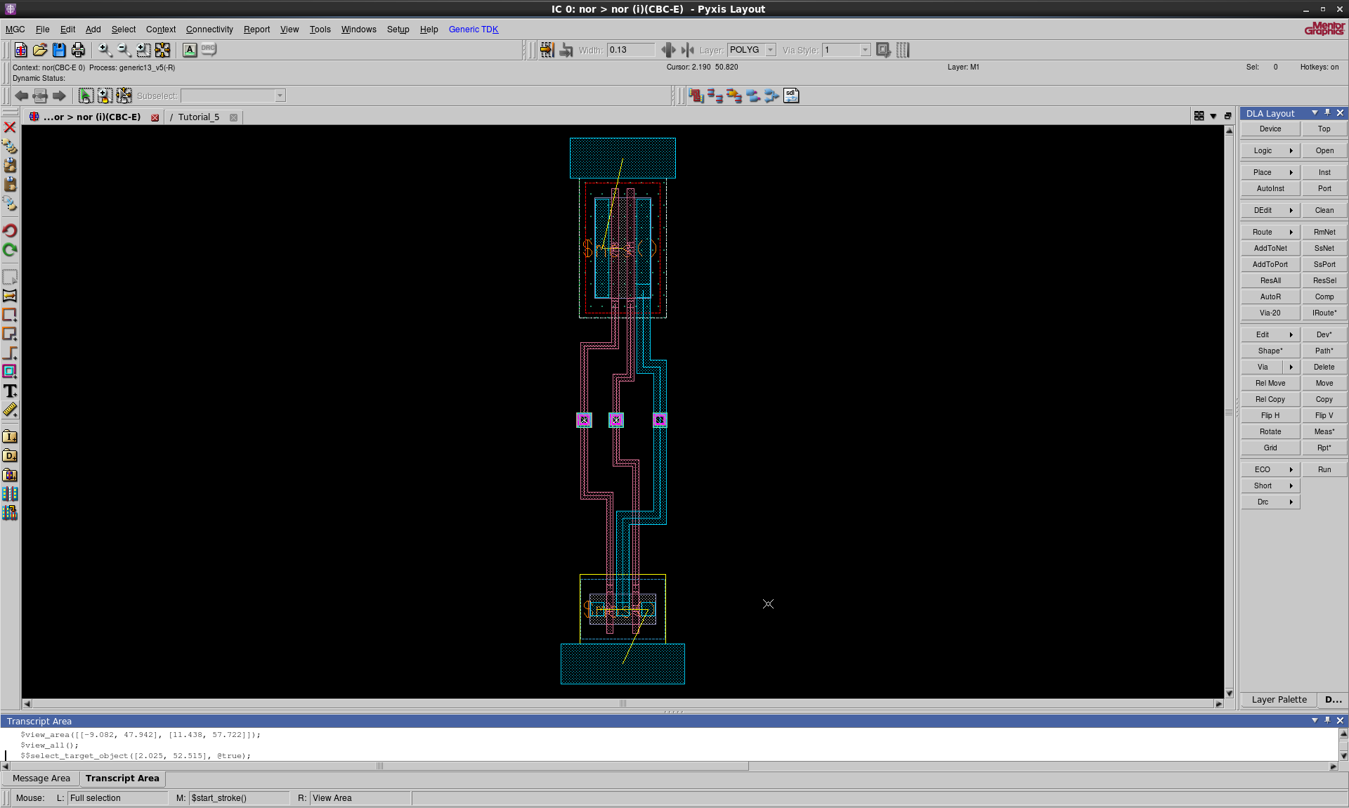
Use iRoute (intelligent router) to connect input 'A' to the transistors. You will need to
create a connection between POLYG and M2. Click on the
iRoute button, then click on the net connected to the gate on the transistor.
Start the POLYG
towards the input and jog over to the left to line up with the Metal 2 "A" port. Close to the "A" port, press 4 twice to move up to Metal 2 (M2) and click on the port. The iRoute router should automatically add the Contact (CO), Metal 1 (M1), and Via 1 (VIA1) shapes necessary to connect from the POLYG layer to the M2 layer of the port.
Repeat using iRoute to route from the other transistor's gate to the "A" input but you will not need to change from POLYG to make the connection to the "A" input.
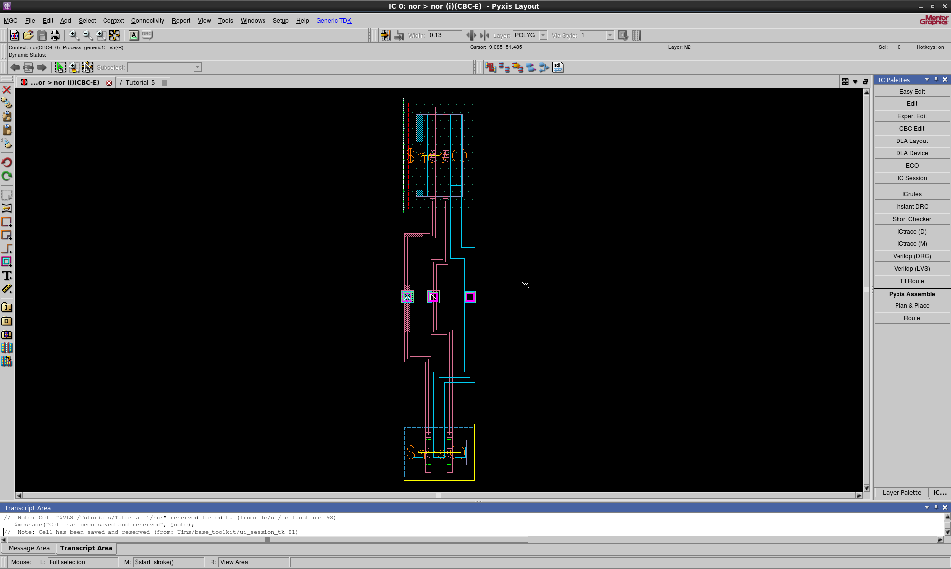
Add input 'B' to the left of input 'A' and the output 'Y' to the right of
input 'A'. Both of those should be Metal 2! Be sure to leave enough space
so there isn't any violation of the rules. Then route the connections as above.
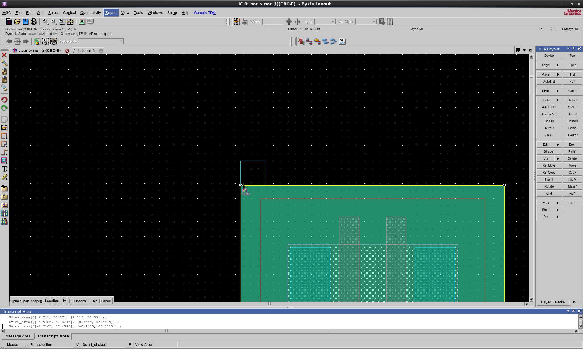
Select the \(V_{DD}\) branch in your schematic and navigate once again to DLA
Logic > Port. Place \(V_{DD}\) (Metal 1) on top of the PMOS
transistor. Align it to the corner as shown below.
Resize \(V_{DD}\) to the width of the transistor and change the height to 0.8
μm. Then, make sure that you've left enough space for two NOR gates to
touch each others \(V_{DD}\) without causing a DRC error because the spacing
between the two would be too small. Hence, make your \(V_{DD}\) wider by the
difference between your out most wire plus 0.09 μm –one way is to access
the properties of the shape by pressing q and modifying the width–moving
(m) the shape and align it to the middle (v). This will allow for two
NOR gates to connect without causing a design rule error because of the
minimum spacing between M1 (0.18 μm). It is also of importance to take
into account the VIA that's going to be added later. Generally the cell
has to have equal width so when you add \(n\) of them next to each other they
align perfectly. Therefore, some trivial calculations have to be done in
order to figure out the optimal width of \(V_{DD}\) and ground–they are
going to be relative to your design. The VIA for \(V_{DD}\) adds 0.26 μm to
the width of the Metal 1. The VIA for
ground adds 0.08 μm to the width of the Metal 1. Assuming that the wire doesn't exceeds the
length of the bigger transistor and that we are taking into account the
biggest transistor for sizing them, the Metal 1 port for the ground node has to be larger by
0.36 μm.
Similarly, connect the ground to the NMOS transistor. Make sure the sizes of VDD and ground are adhering to the specifications above.
Navigate to DLA Layout > Via > Fill Selected fill \(V_{DD}\) with m1nwell
VIA and ground with m1psub VIA .
Finish by routing the rest of the circuit and add text to ports
(Connectivity > Add Text on Ports... > OK).
Run DRC as in previous tutorials.
DRC will yield six errors. Two of those errors are M1.A.1 errors:
M1.A.1 { @ Min. M1 area region 0.122 um*um


  AREA M1 < 0.122


}
You can select this error in the DRC results window, right click and select Highlight. It will show the errors refer to the M1 shapes around the "A" and "B" inputs. Those M1 shapes do not have the minimum area and since they will remain as they are inside the cell, they must be fixed.
Create an M1 shape that has a height and width of 0.35um and place it on top of the "A" and "B" inputs as shown below.
Run code>DRC again and you should get 4 errors as the M1.A.1 errors should be fixed.
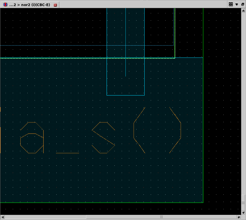
Three of the errors are M2.A.1 errors - one each on ports "A", "B", and "Y".
M2.A.1 { @ Min. M2 area region 0.144


AREA M2 < 0.144


}
If you Highlight those errors, you should see them as shown below.
These arrors will be fixed when we wire up the M2 ports to Metal 2 wires when we connect up the cells, thus we can leave those as is for now.
The other remaining error is PO.R.2. This error has to do with how much POLYGthere is in the
layout. Simply there isn't enough, which as we know, would cause problems during the CMP process. However, you can disregard this error since we are not actually going to fab our design. However, this is the ONLY error that can remain in your design in order for it to be considered correct.
The final step is to put a floorplanning layer (fp1) on the cell to mark the exterior extent of the cell. This step is optional, but it is HIGHLY recommended.
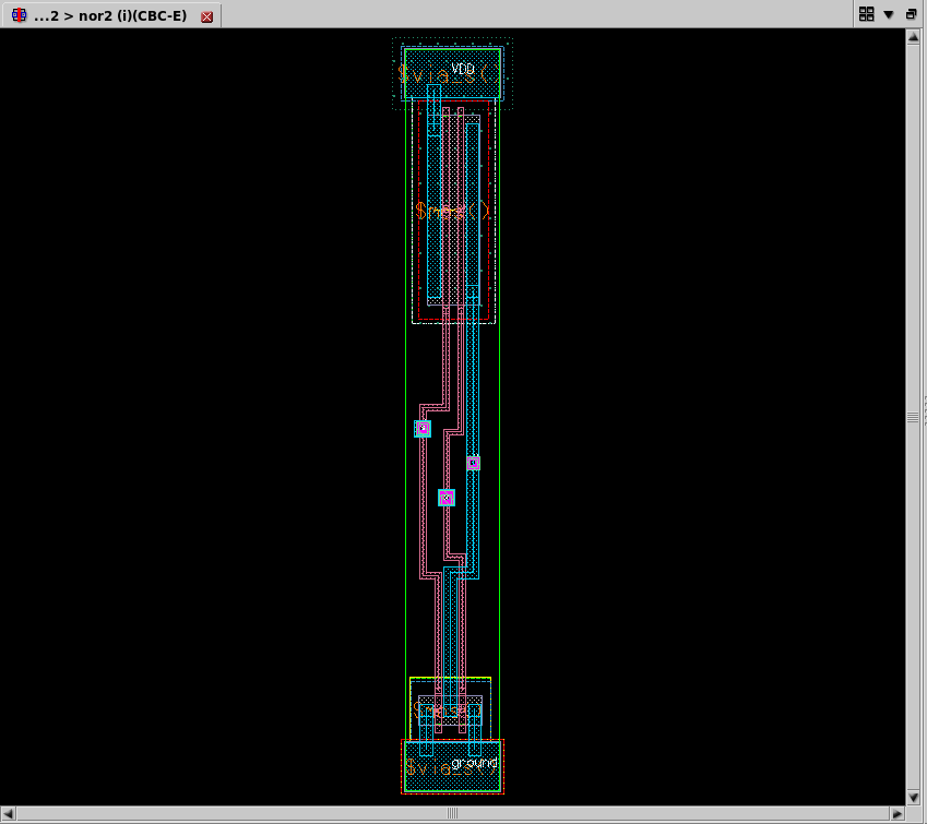
Place the fp1 shape around the cell starting at the top left corner of the M1 VDD shape, and ending at the bottom left corner of the M1 ground shape. Adjust the fp1 shape carefully so that it lines up with the M1 VDD and ground shapes EXACTLY. Remember that the minimum grid spacing is only 0.005um. Getting this exactly right at this point will make it much easier and faster to layout your blocks out using your cells later. The result should be as shown below.
Once you've laid out the fp1 shape, the result should look something like this. Notice that the nwell and n+ and p+ shapes extend past the edges of the cell, but that is OK.
In the menus, select the View->Show Contest->Aspect: item. In the dialog box that comes up, select external and click Ok. Your layout should look like this:
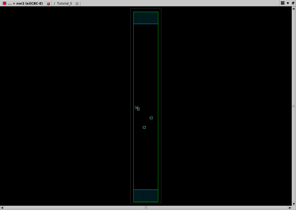
This is the view you will have of your NOR2 cell when you instantiate it in a higher level block. Notice how you can see the VDD and ground ports in M1, the A, B, and Y ports in M2, and the outside extent of the cell in the fp1 layer.
Select the View->Show Contest->Aspect: item and select internal and click Ok. Your layout should go back to the view you had before.
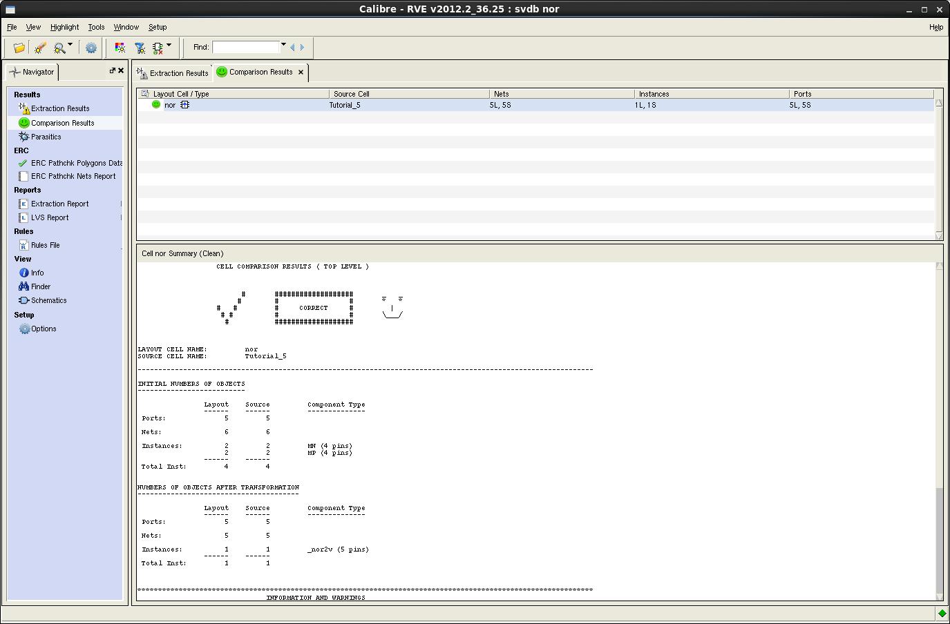
Run LVS as in previous tutorials. The cell should pass LVS checks.
Save your layout and exit Pyxis Layout. Finally, extract the SPICE file
as per Tutorial 3, make a "do" file, and simulate the NOR gate to verify
its correct operation.