IV. Full Custom IC Design Using Device Generators
Table of Contents
Introduction
In this tutorial we will use Pyxis Layout to create a CMOS inverter. In Tutorial 2 we created an inverter by drawing every individual polygon. This time we will use the MOS device generators to quickly draw the required transistors.
Prepare your Workspace
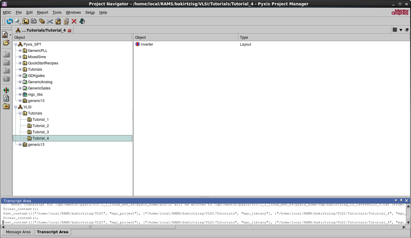
Add a cell to your Tutorials named Tutorial_4 and create
a layout called inverter.
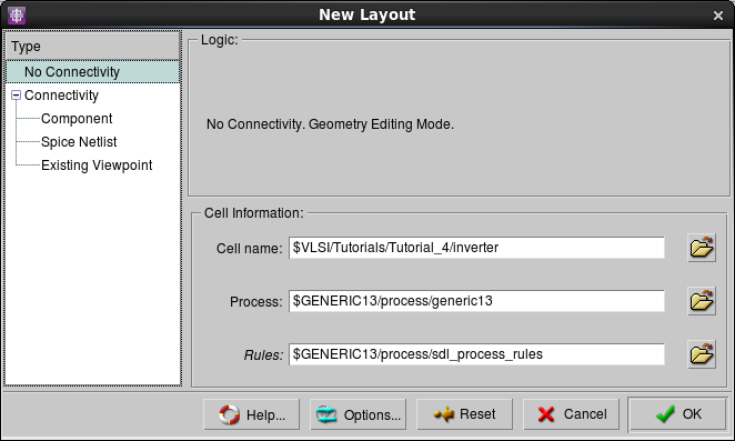
Create a new layout that uses the generic13 process and has No
Connectivity.
Adding the Transistors Using Device Generators
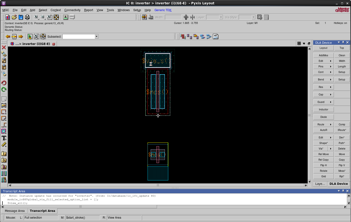
Navigate to DLA Device > AddMos. Add the component to your layout.
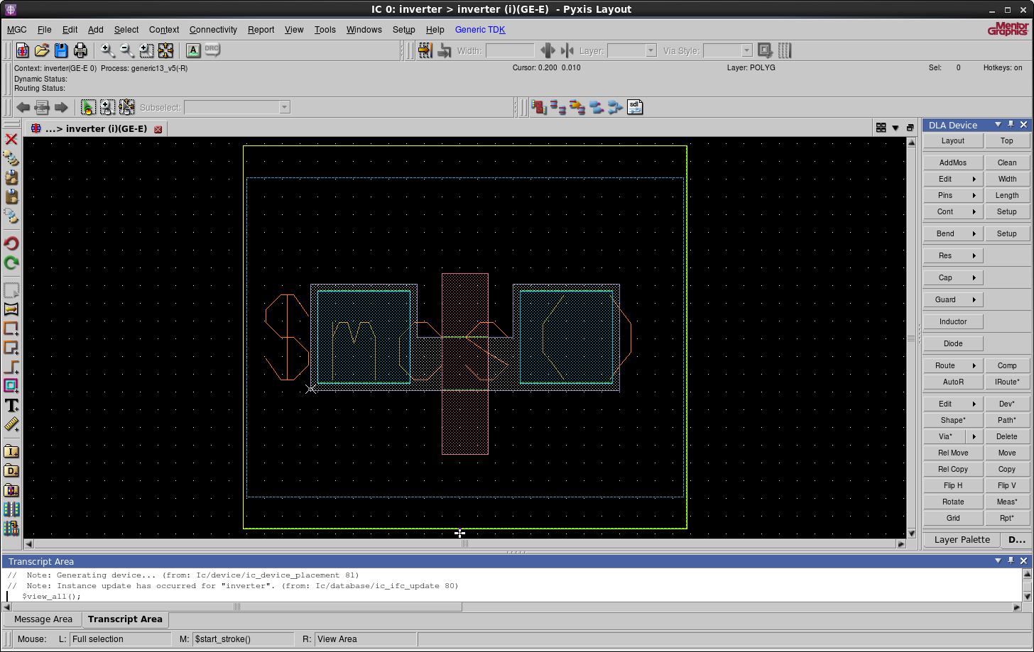
Press ESC and select the component then access it's properties by
pressing q. Change the mos type to pmos and the finger width to 2 μm.
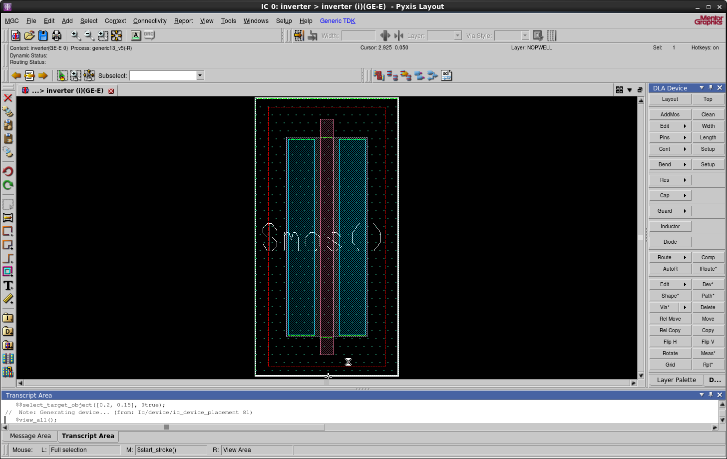
Similarly add another MOSFET of n-type and change the width to 0.6 μm. Then
press ESC, select the object, press m to move it. While you're moving
it press v to invoke the align function and align it in the middle of the
PMOS transistor.
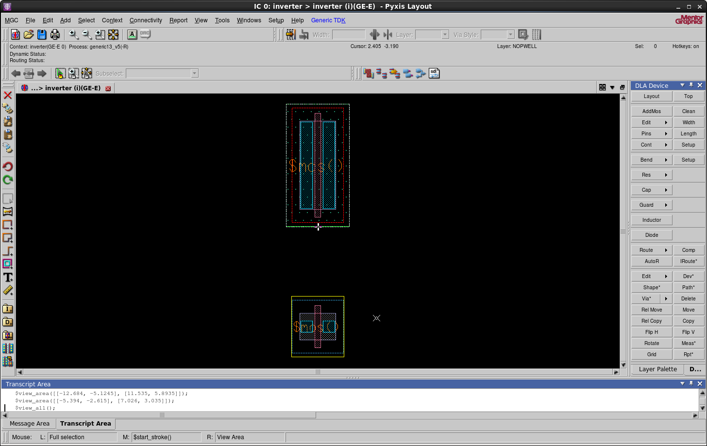
Remark: The Sequence parameter tells the device generator what
combination of polysilicon gates and contacts you want in the
transistor. For this case, the default is cgc, which means
contact-gate-contact. For a diffusion shared string of three transistors
the sequency would be cgggc (e.g., contact-gate-gate-gate-contact). You
can have any arbitrary sequence of gates and contacts and also specify a
different width for each transistor by putting a comma separated list of
numbers in the width field.
Creating the Positive Supply Voltage and the Reference Node
Lay a Metal 1 shape on top of the PMOS transistor – there should be no
spacing between the two. Invoke the s command
to resize your shape to the width of the transistor. It might be useful to
use align (v) while resizing to make sure it is exactly on
top of the PMOS transistor. On that note, remember that you can use m to move the
shape wherever you want. Finally change the height of the Metal 1 to 0.8 μm.
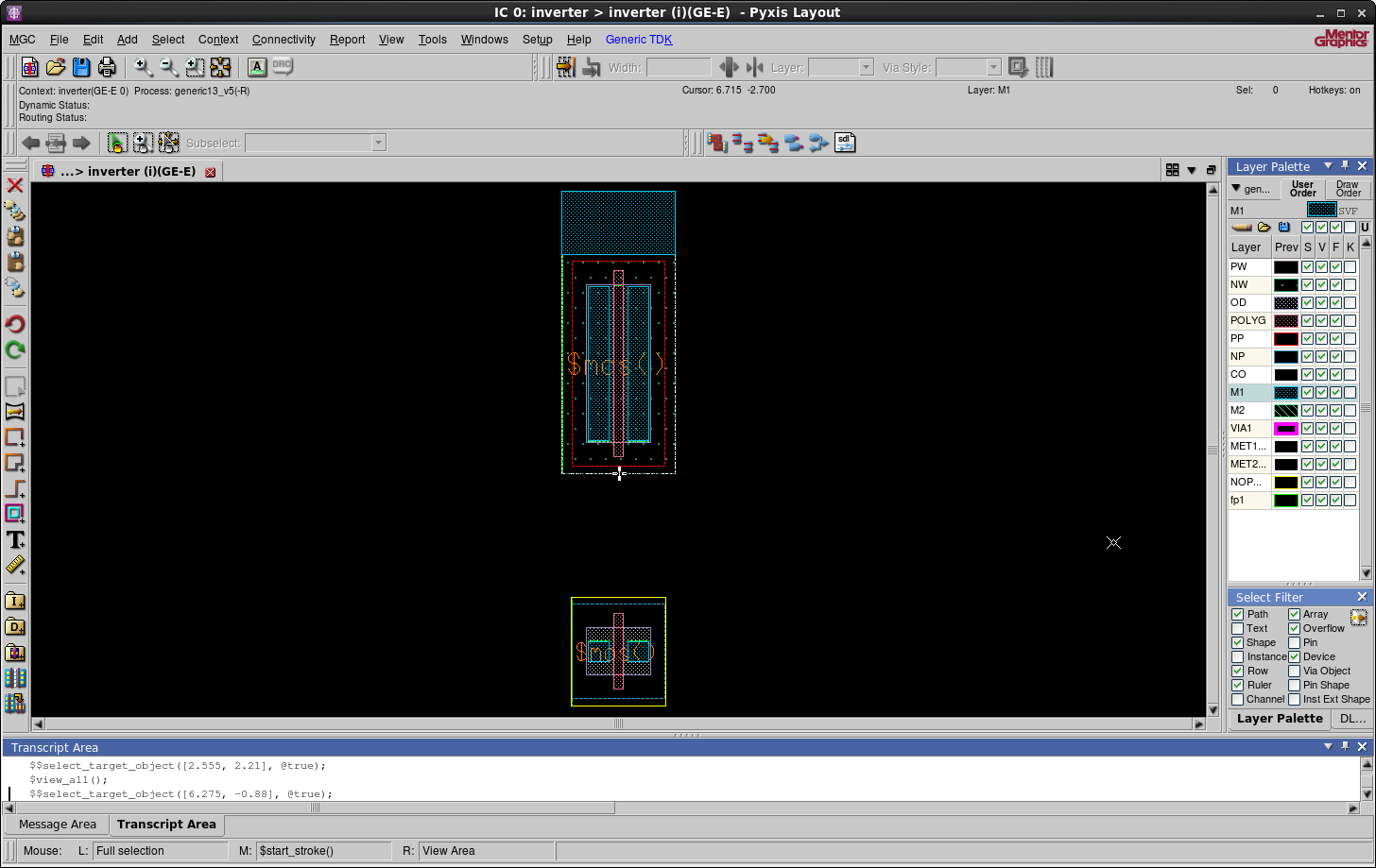
Similarly make the ground under the NMOS transistor.
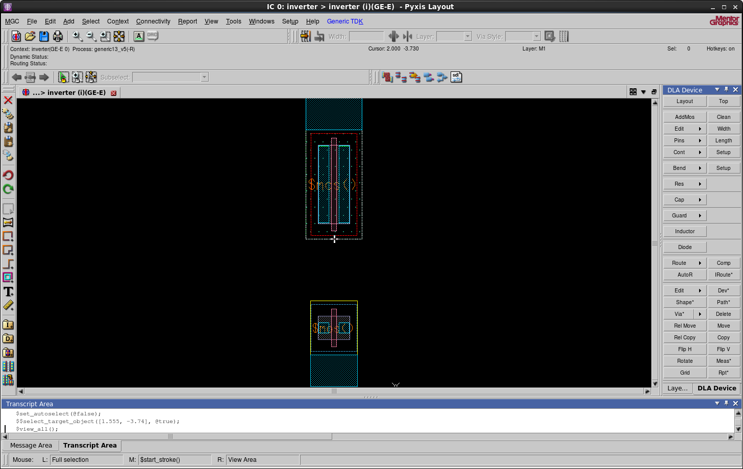
Select the Metal 1 corresponding to \(V_{DD}\) and navigate to DLA Device >
Via* > Fill Selected. Choose m1nwell.
Select the Metal 1 corresponding to ground and fill it with m1psub.
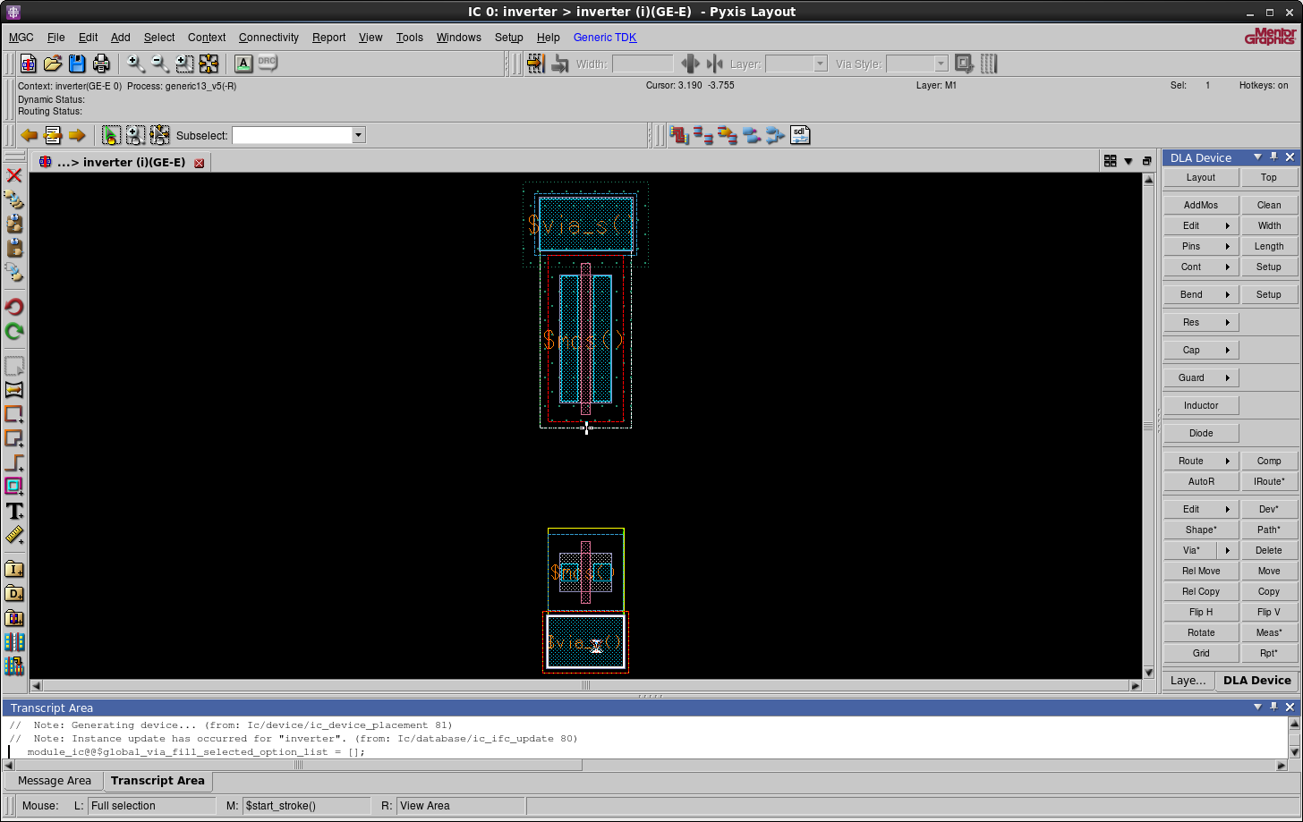
We have successfully created the positive supply voltage and the reference node of our circuit. Remember to run DRC during the design of the circuit.
Finishing the Circuit
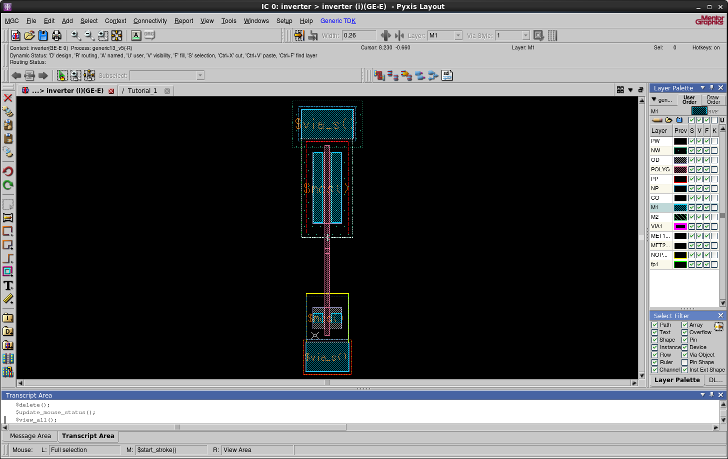
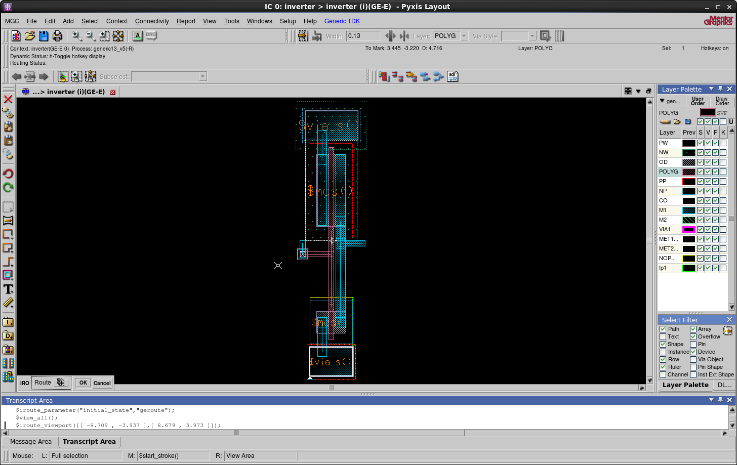
Instead of creating shapes or paths to make the necessary connections we will instead
use the IRoute function to route the circuit

Click on the IRoute icon as shown above. You can change layer type by
pressing 3 to go down a level or 4 to go up a level. Using that
information connect the POLYG of the PMOS transistor with the NMOS
transistor.
Connect the NMOS with the ground, the PMOS with \(V_{DD}\), as well as the
Metal 1 of the NMOS transistor with the PMOS transistor. Shift+w will
automatically change the width of the Metal 1 to the correct size. Simply,
start laying the path and press Shift+w.
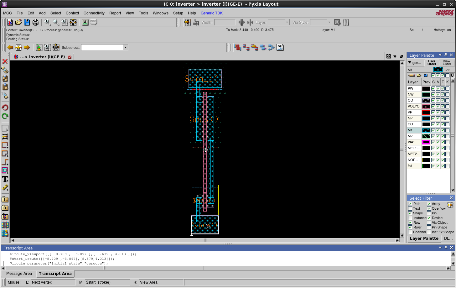
Make the input and output paths with Metal 1.
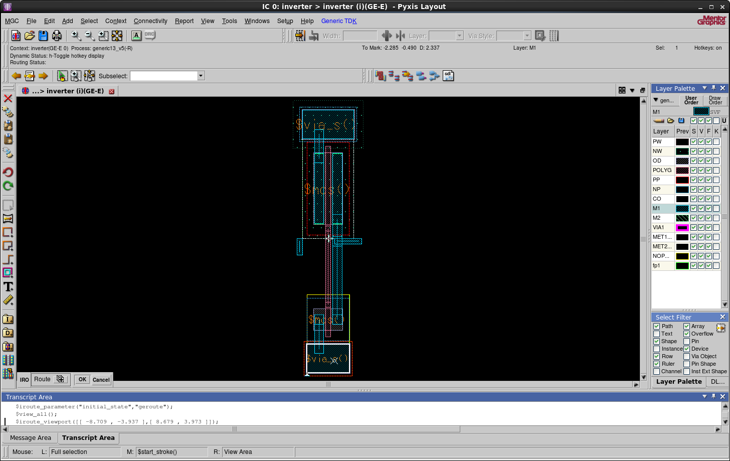
Finally connect the POLYG with the Metal 1 of the input. Be sure that
IRoute is set to POLYG lay the path towards the input node. Press 4,
in order to go to Metal 1, while still laying the path to make the necessary
connection between the two.
We've successfully routed the circuit. Make the necessary ports and add text to them as before.

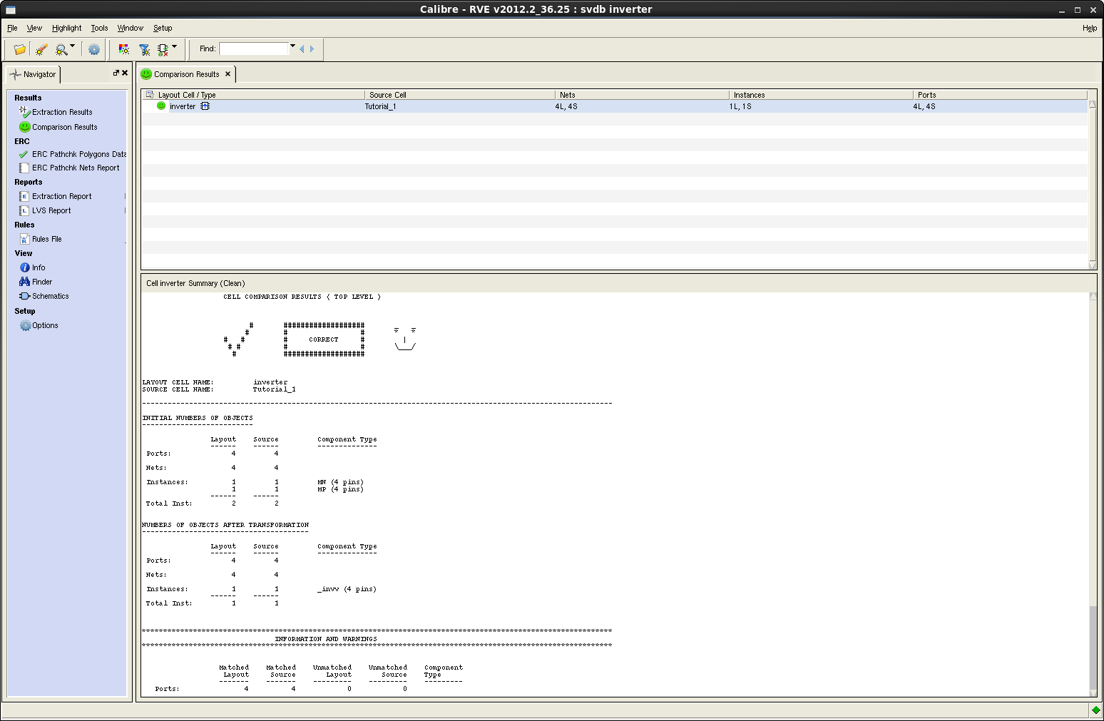
Run DRC to check for any warnings. If necessary adjust the circuit accordingly. Finally save your cell run a Layout vs. Schematic (LVS) using the schematic from Tutorial 1.