I. Transistor-level Design and Functional Simulation with Pyxis
Table of Contents
Introduction
In this tutorial we will use the Mentor Graphics Pyxis Design Suite to construct an inverter. The transient response and the dc switching characteristics of the resulting schematic will be simulated to verify the correct operation of the inverter.
Useful Shortcuts for Pyxis Schematic
F2: Deselect everything.ESC: Terminate the current operation – use to quit adding wires or elements.DEL: Delete a selected element.u: Undo previous actions.q: Accesses the properties of the element hovered over by the cursor.Shift+F7: Change text hovered over by the cursor – used to change net names, port names, and widths.Shift+F8: Zoom to fit window.Numeric Pad +: Zoom in.Numeric Pad -: Zoom out.Page Up: Move window up (e.g., object down).Page Down: Move window down (e.g., object up).CTRL+Page Up: Move window left (e.g., object right).CTRL+Page down: Move window right (e.g., object left).
Opening Pyxis Project Navigator
Open a terminal (Applications > System Tools > Terminal) make an
EGRE591/VLSI folder in your home directory:
$ mkdir EGRE591
$ mkdir EGRE591/VLSI
Use the built-in script to copy the Mentor Graphics Generic Design Kit files into your home directory and uncompress it.
$ setupGDK.sh
$ cd GDK/Pyxis_SPT_HEP
$ ./setup_Pyxis_SPT
You will need to do the above steps to copy the GDK folder and run setup_Pyxis_SPT every time you use
a different workstation.
Then open the Pyxis Design Manager by executing open_Pyxis_SPT:
$ ./open_Pyxis_SPT
Note that if you log into a workstation that already has the GDK setup in your home directory, you can open Pyxis Design Manager by executing open_Pyxis_SPT without doing the preparatory steps above.
Prepare your Workspace
In the Pyxis Project Navigator go to File > New > Project. In the Project path, select the EGRE591/VLSI folder. Left click on Derive Settings from Existing Project.
The final setup should look like the one below. Press OK.
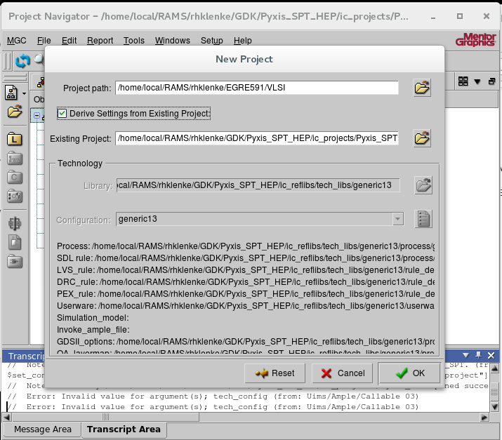
We will only need the library generic13 so you can remove the rest of the
libraries then press OK.
This is where all your files for the semester will go.
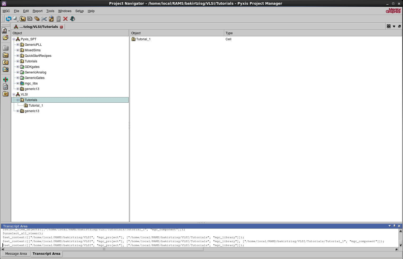
Right click on the VLSI object then select New
> Library. Name the new library Tutorials and press OK.
Similarly, right click on Tutorials libary then select New > Cell. Name
the new cell Tutorial_1 and press OK.
Make sure you keep this folder neat by creating a new cell for every
tutorial. Also, in order to maintain your files, copy your class folder
(e.g., EGRE533) to a flash drive before you log out of the computer. That
way when you change computers you can just copy the class folder to your home
folder and work from where you left off.
Remark: In order to open your project after you copy the folder in your home navigate
to File > Open > Hierarchy and choose the VLSI folder in EGRE533.
Creating a Schematic of a CMOS Inverter
Right click on Tutorial_1 then select New > Schematic. Name the
schematic inverter and press OK. This will open an empty sheet in
Pyxis Schematic.
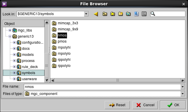
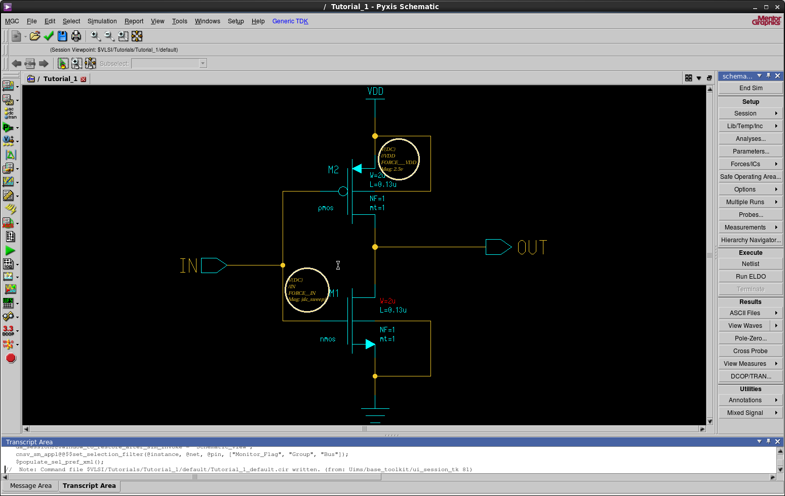
Navigate to Add > Instance... > Choose Symbol. Under generic13 > symbols
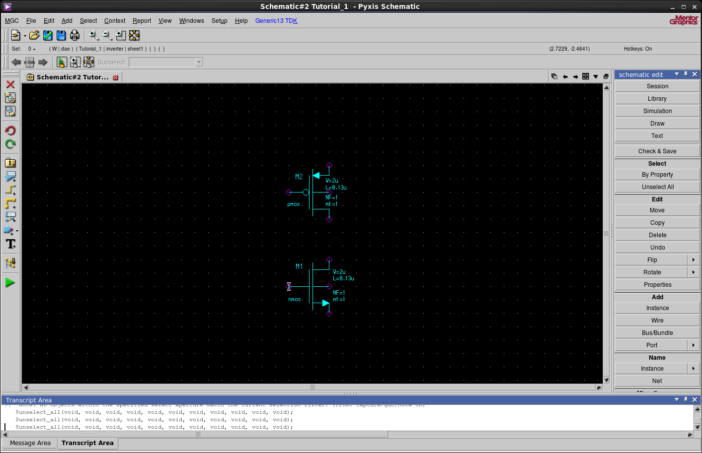
add the PMOS and NMOS elements to your schematic.
The schematic now should look like the one below.
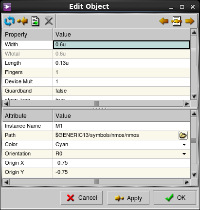
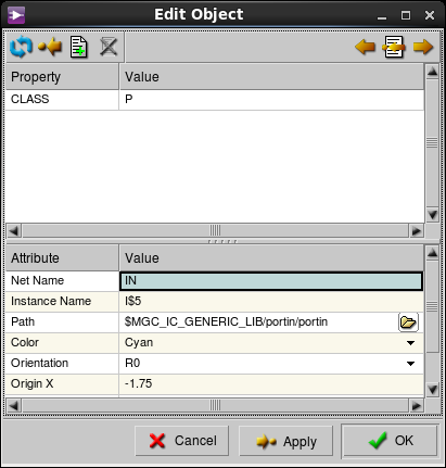
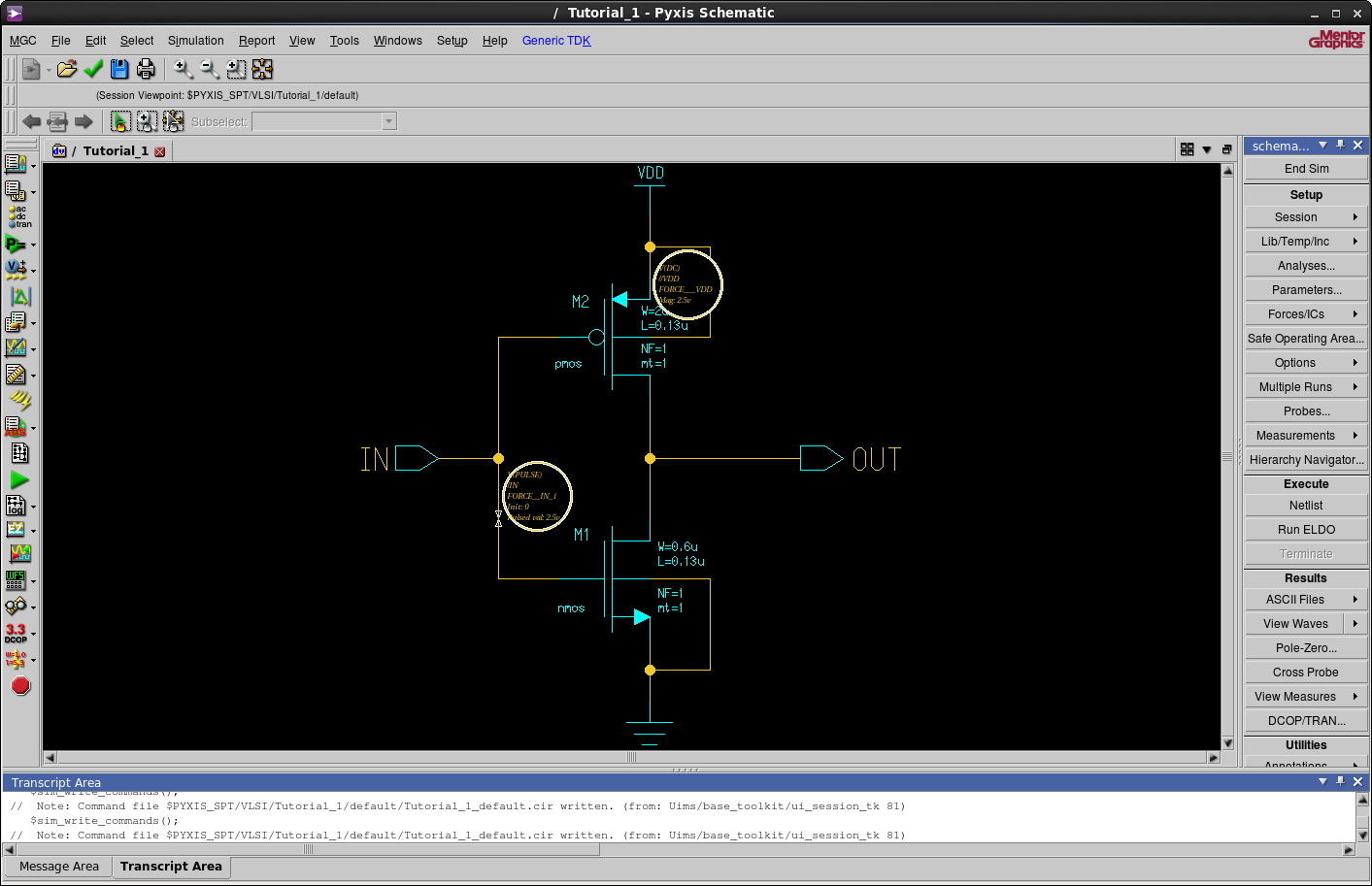
Select the NMOS and press q. This will bring up the Edit
Object window. Change the width to 0.6 μm.
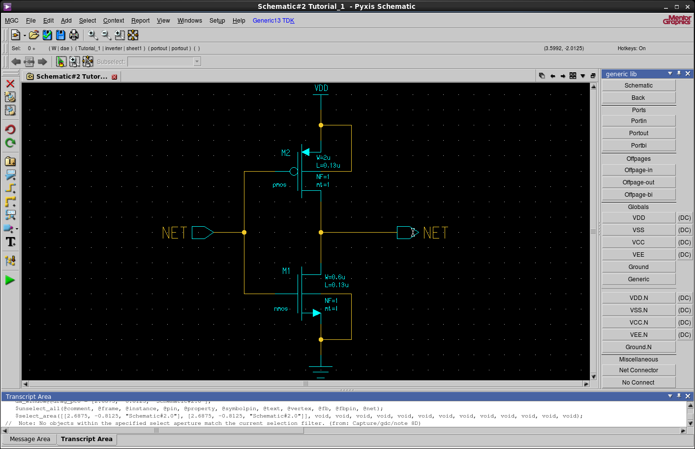
In the Schematic Edit located to the right navigate to Library > Generic Lib. There
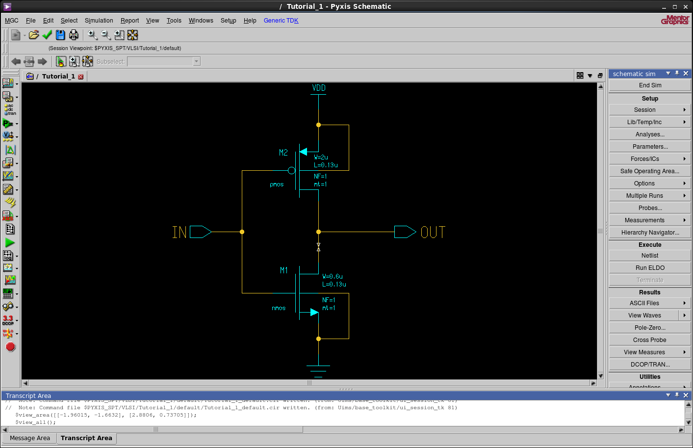
you will find VDD, ground, portin, and portout. Add these elements to your
schematic as shown below.

Add wire by pressing w and choosing the starting node. Lay the wire to
the desired ending node. After you choose the ending node you might need to
press ESC to stop the Add Wire function.
Hover over the input and output ports and press Shift+F7. Change the
names to IN and OUT accordingly.
The final schematic should look like the one below.

Check and save the sheet (Ctrl+S), fixing any errors, before you proceed
to the simulation.
Simulation of the Transient Response of the Inverter
Go back to the IC Library to the right and left click on
Simulation. In the next window just click on OK. You should now be in
simulation mode.
Before we run the simulation we will need to perform a little setup work for the simulator to operate properly.
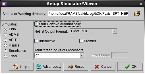
Navigate to Setup > Session > Simulator/Viewer.... Make sure that ELDO
is the selected simulator. Also, check Start EZwave automatically.
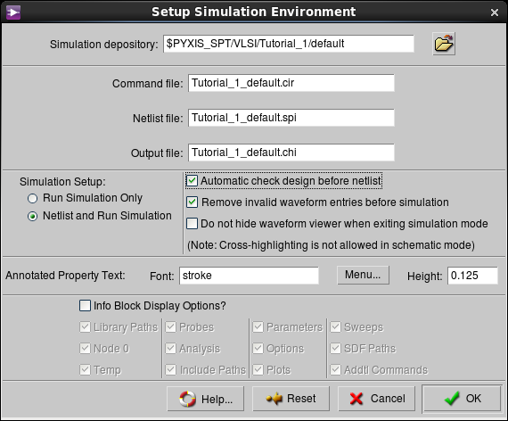
Navigate to Setup > Session > Environment. Make sure "Automatic check
design before netlist" is chosen as shown below.
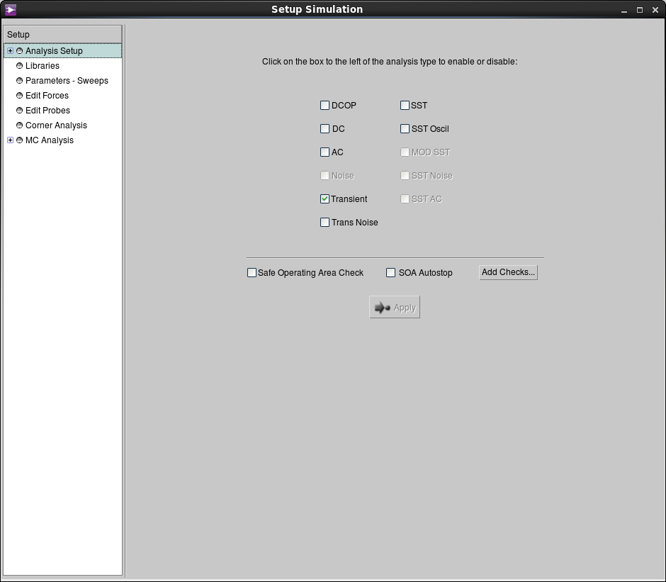
Left click on Analyses and choose Transient then left click Apply.
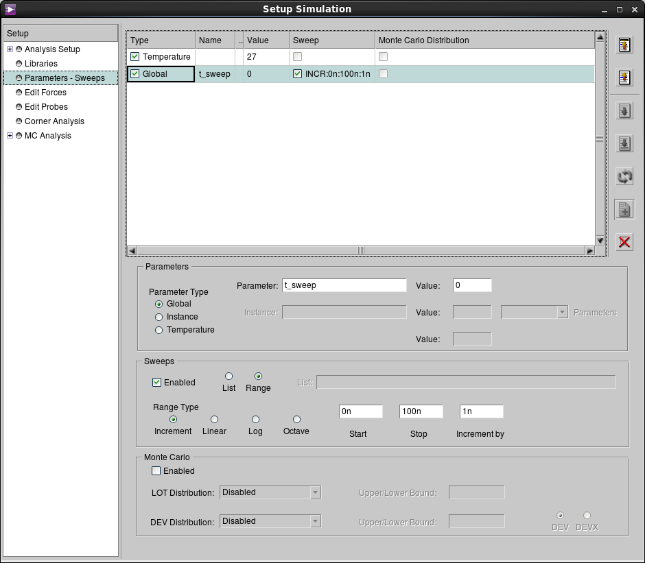
Navigate to Parameters - Sweeps. Add a parameter t_sweep, as shown below, to set the
step and the stopping time of the simulation.
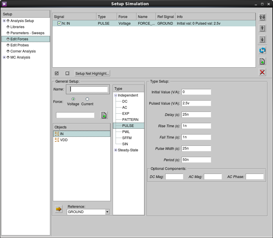
At this point it's necessary to define an input wave. Select IN on the
schematic and navigate to Forces > Manager. Add a pulse input waveform
with the attributes shown below. The input will be a pulse which starts
low (0 V) at time 0 second then pulses high (2.5 V) 25 nanoseconds later and repeats
at 50 nanosecond intervals. The rise time and fall time of the pulse will
be 1 nanosecond. Since the stop time is set by default at 100 nanoseconds,
you should see two pulses.
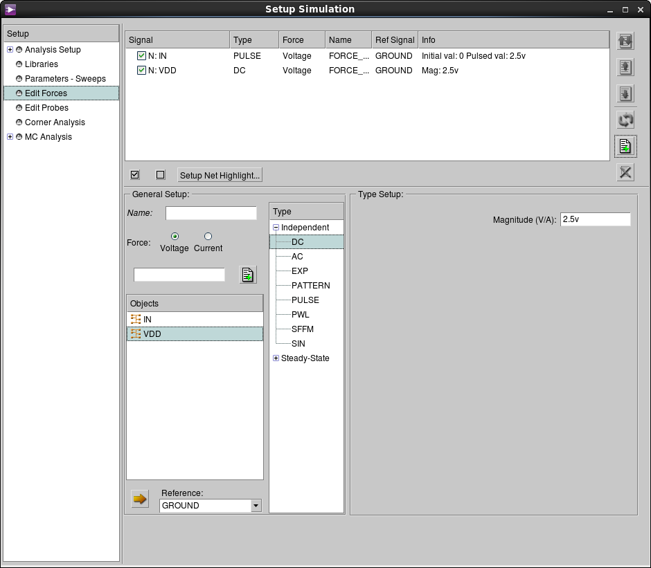
Similarly, select the VDD branch and navigate to Forces > Manager. Set the magnitude
of a DC force to 2.5 Volts.
You should now see the forces on your schematic in simulation mode as shown below.
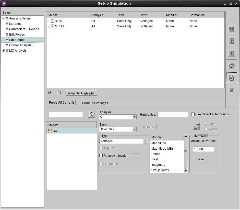
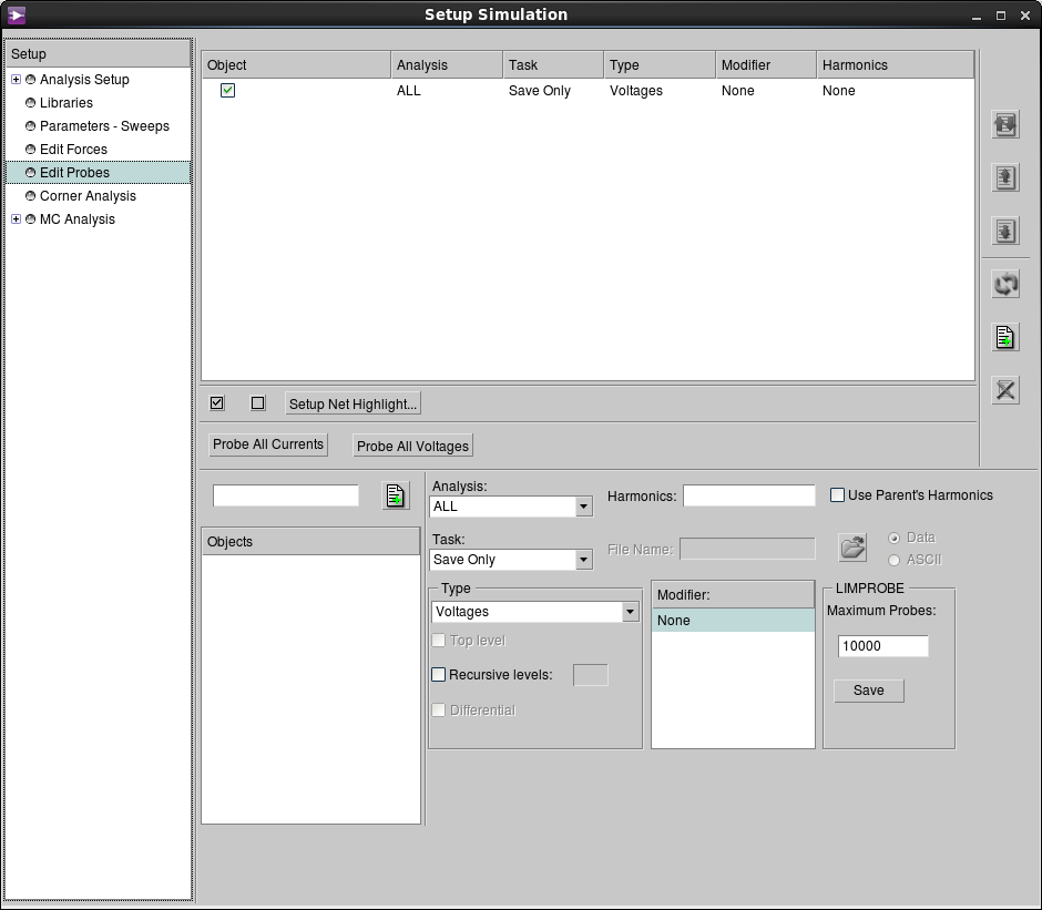
Click on the input branch and navigate to Setup > Probes add the input
signal to be plotted in the simulation. Similarly add the output
signal. The resulting setup should look like the one below.
Finally run the simulation by clicking Run ELDO under Schematic Sim >
Execute (note that ELDO is the name of the simulator). The results of the
simulator will open in a separate application EZwave. If EZwave doesn't
launch automatically, navigate to Schematic Sim > Results and left click on
View Waves.
In the event that the voltages didn't plot correctly close that
window inside EZwave and navigate to Tutorial_1_default > DC. Choose both
V(IN) and V(OUT), right click and choose Plot (Stacked).
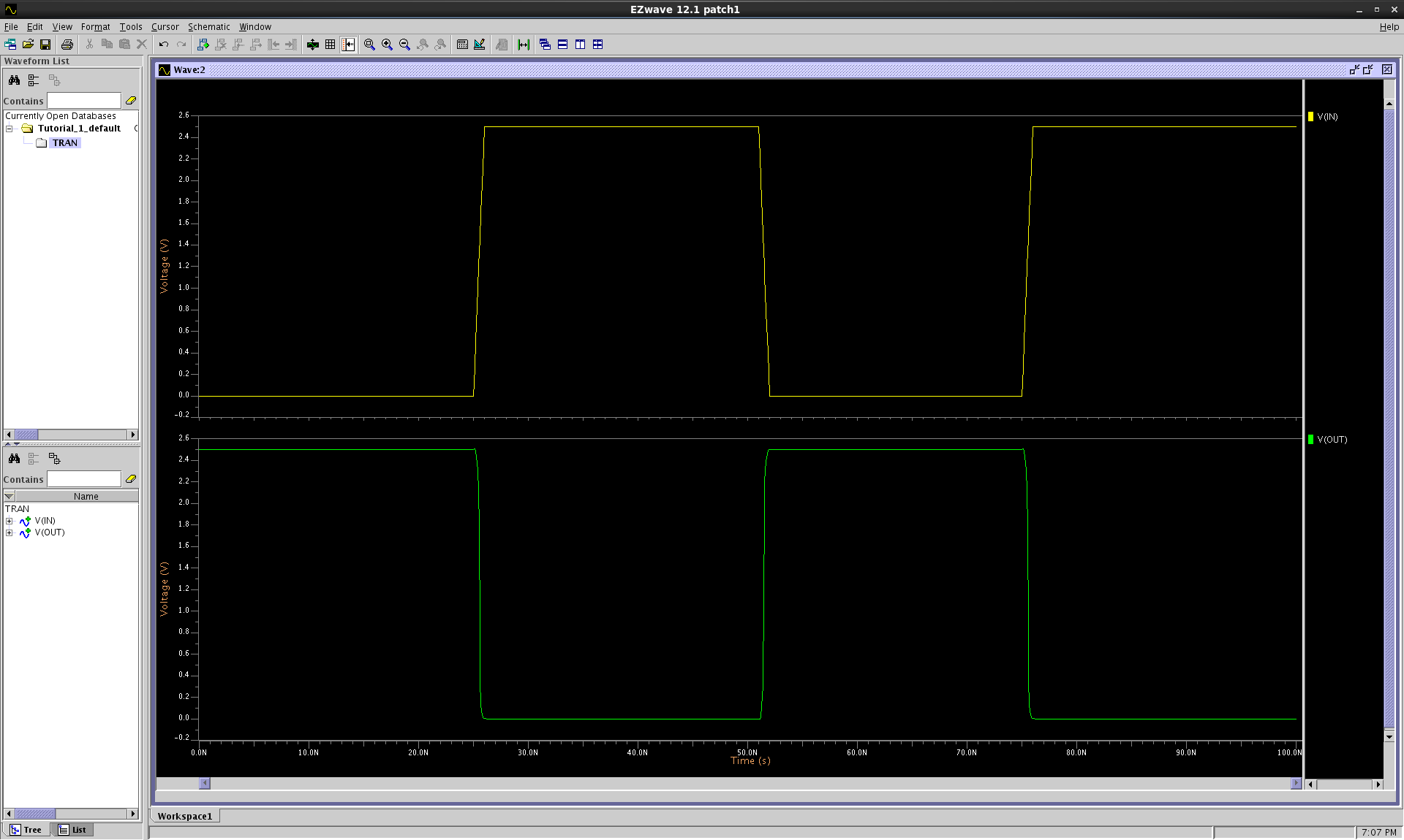
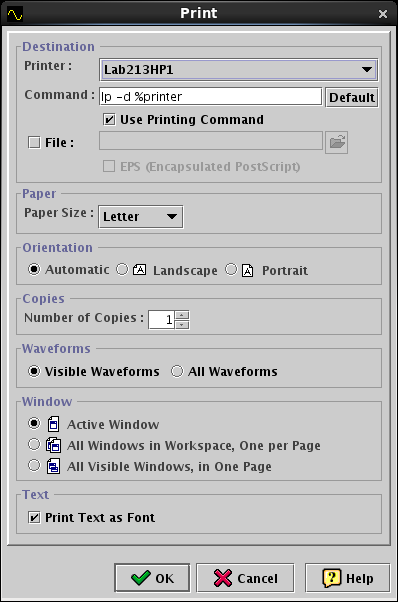
Select File > Print in EZwave to print your simulation results that
verify the correct operation of the inverter. Then close EZwave.
Remark: If you do not see the waveforms shown above close EZwave and in Pyxis
Schematic navigate to Schematic Sim > Results > ASCII Files then click on
View Complete Log. This will open a notepad window containing the log file
of the simulation and it's parameters. You can read the log file to locate
errors. Correct your errors and run the simulation again.
Simulation of the Switching Characteristics of the Inverter
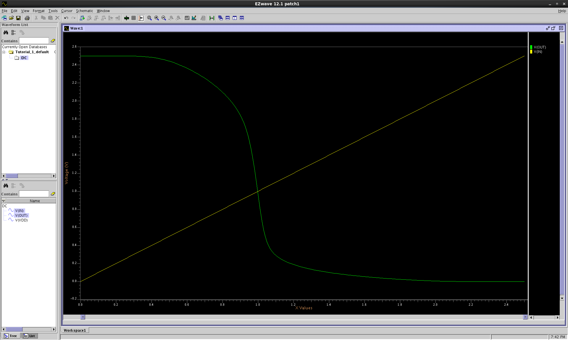
Now we will simulate the DC switching characteristics of the inverter. You will program the simulator to sweep the input voltage from 0 V to 2.5 V and plot the resulting output voltage. This plot of \(V_{OUT}\) vs. \(V_{IN}\) will show the switching threshold and noise margin of the design.
First you will need to remove the forces and the probes that were created to simulate the transient response of the CMOS inverter.
Delete each force by navigating to Schematic Sim > Forces/ICs >
Manager. Select each force and press DEL.
Delete each probe by navigating to Schematic Sim > Setup > Probes. Select
each probe and press DEL.
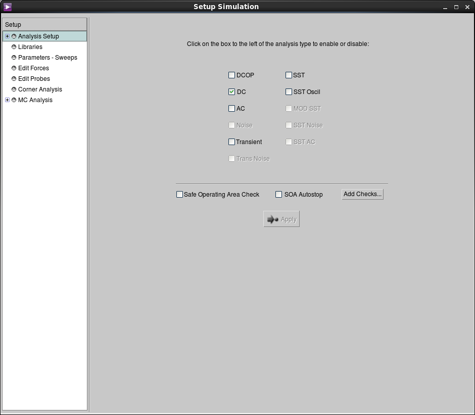
Navigate to Setup > Analyses .... Deselect the Transient and select
DC.
Navigate to Parameters - Sweeps. Remove the t_sweep parameter by left
clicking and hitting DEL.
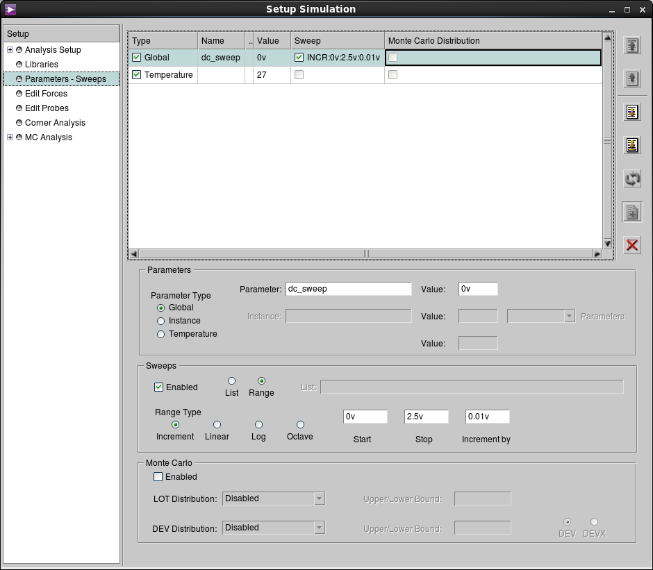
Add a dc_sweep parameter that will define the voltage range and the step
of the sweep. The values should be from 0 V to 2.5 V with a step of 0.01 V.
Choose the VDD branch and navigate to Schematic Sim > Forces/ICs >
Manager and add a DC force of value 2.5 V.

Add a DC force of value {dc_sweep} to the input signal.
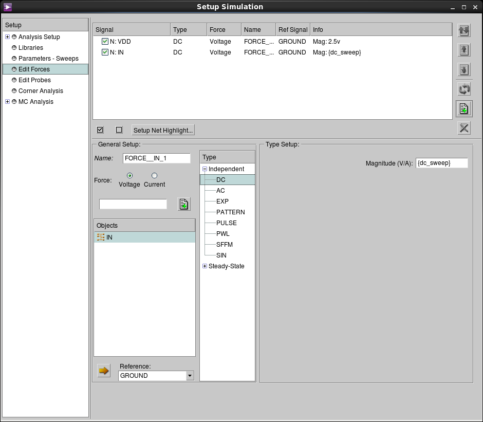
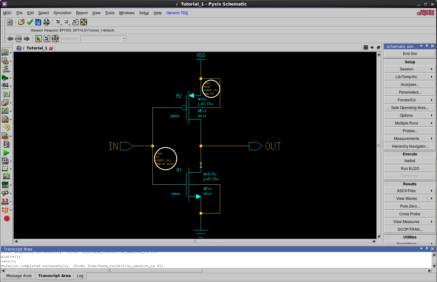
The resulting schematic with the added forces should look like the one below.
Navigate to Schematic Sim > Probes... and left click on Probe All
Voltages.
Left click on Run Eldo as before. EZwave should open
automatically.
As before we want to plot the input and the output of the inverter. In this
case it makes more sense to plot both signals on the same plot since it's
the convention for viewing transfer characteristics.
If the voltages didn't plot correctly close that
window inside EZwave and navigate to Tutorial_1_default > DC. Choose both
V(IN) and V(OUT), right click and choose Plot (Overlaid).
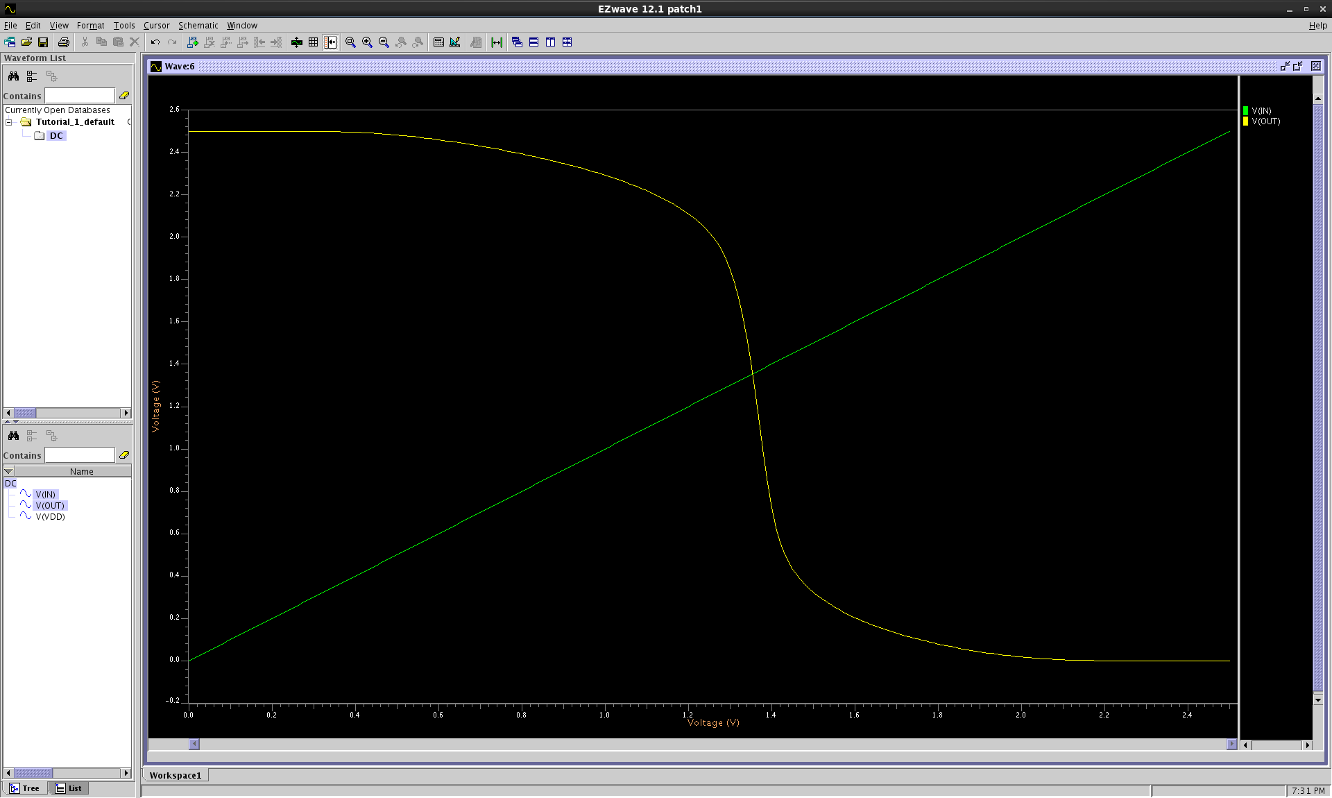
In the beginning of the tutorial we changed the width of the NMOS transistor to 0.6 microns (u). This was done in order to create a balance between the strength of the PMOS and the NMOS transistors. By doing so, the above graph has a crossover point of \(V_{IN}\) and \(V_{OUT}\) that is essentially \(\frac{V_{DD}}{2}\).
It is importance to realize that if this fundamental change to the width of the NMOS transistor wasn't made initially, the graph of \(V_{OUT}\) vs. \(V_{IN}\) would look different.
Close EZwave and change the NMOS transistor width back to 2 μm in
simulation mode.
Run a DC analysis once again. You should now notice that crossover point of \(V_{IN}\) and \(V_{OUT}\) occurs at a lower voltage than before, less than \(\frac{V_{DD}}{2}\).