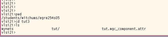
2) In general, create a separate directory for each design you make. In this case, use a Console or Terminal to create a new directory for this tutorial then change your working directory to this new directory and startup Board Architect:
vlsi01> mkdir tut3
vlsi01> cd tut3
vlsi01> ba &
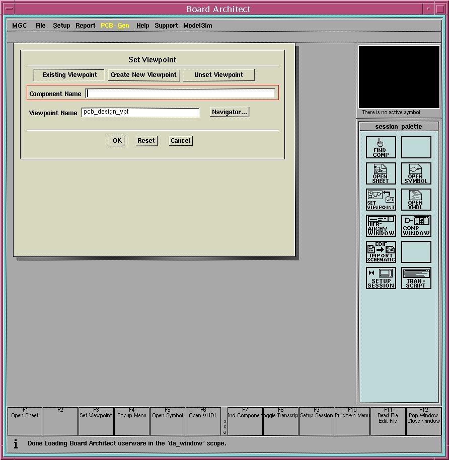
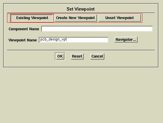
3) Use the File->Open->Set Viewpoint command (or the Set Viewpoint icon on the menu) to create a new viewpoint into your design. Your screen should look like this:
4) You want to create a new viewpoint for your design (a viewpoint is the portal through which the Mentor software sees your design). Type in tut for the name of the design and select PCB for the type of viewpoint. Your screen should look like:

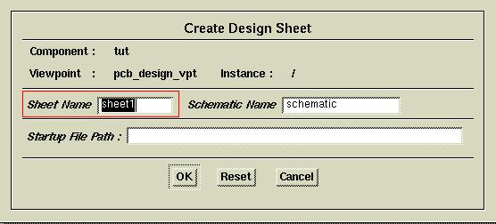
5) Select OK. Next you will see another popup window for creating the first sheet in your design. Leave the Sheet Name as sheet1. Select OK in this window as well.
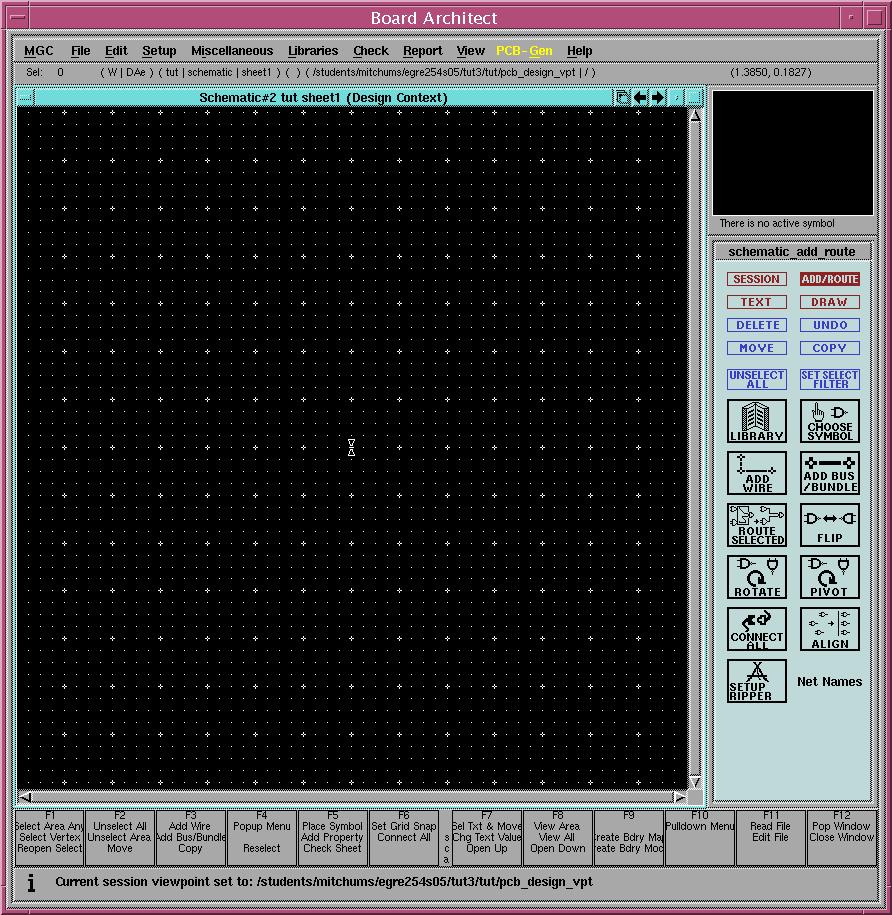
6) Board Architect is very similar to Design Architect - the
difference is you would use Design Architect if you will implement your
design in an ASIC or FPGA but you would use Board Architect if you will
prototype your design using logic chips or your will implement your design
as a PCB. Your screen should now show a blank schematic page and
the default library palette like this:
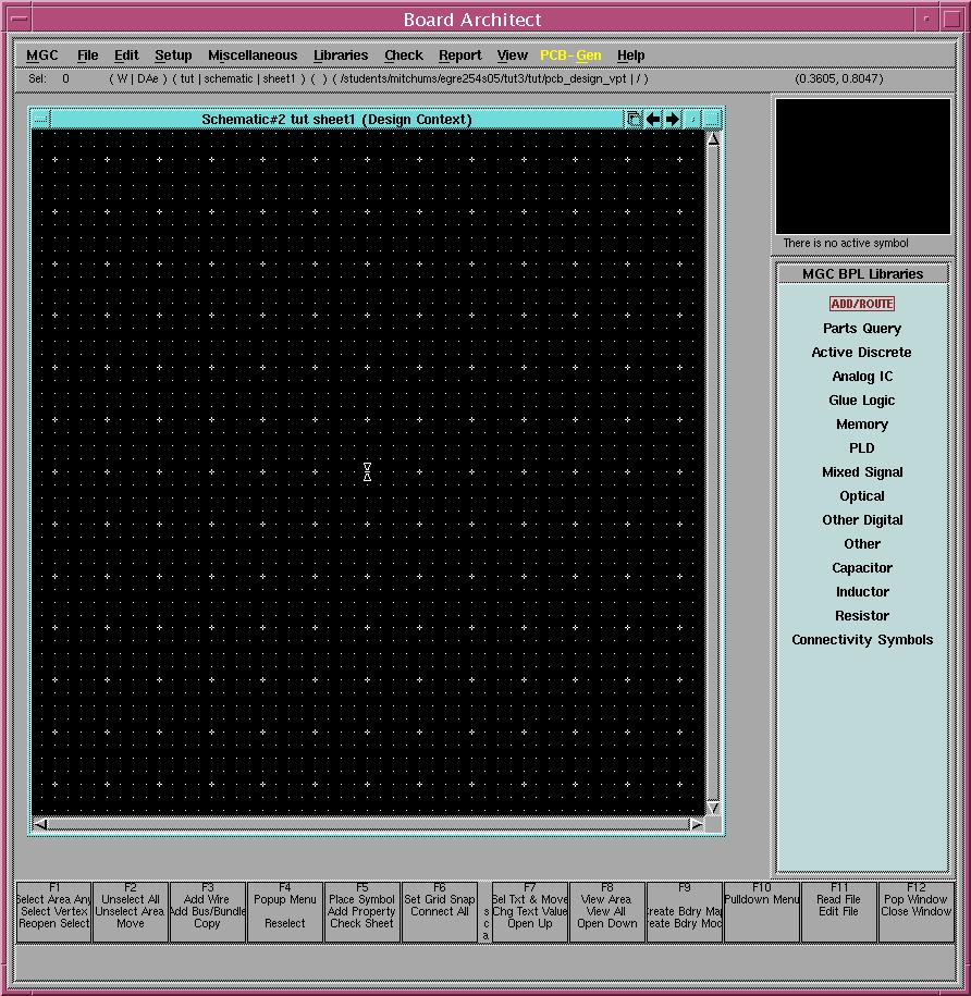
7) To get 74LS logic parts, we need to open the appropriate library. Left click once on Libraries in the top menu bar. Then left click once on MGC Board Process Libraries in the pull down menu. Your screen should now look like:
8) Now to get the 74LS parts, select Glue Logic. All the standard logic parts like inverters, nand gates, nor gates and flipflops are considered glue logic by Board Architect. You will get a menu of available digital part families. The menu should look like:
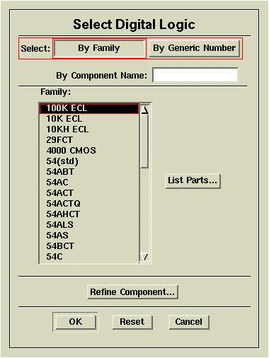
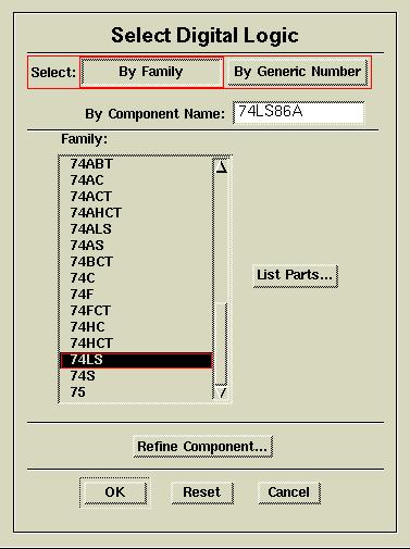
9) From within this menu select 74LS in the scrolling window. Then click once on the List Parts button. You will see a new menu listing all the 74LS parts in the system:

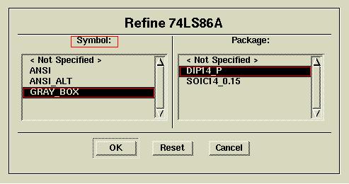
10) Highlight 74LS00 (NAND gates) and then click OK once to return to the Select Digital Logic menu. Then click the Refine Component... button to define the package and symbols. You must use Refine Component if you want Board Architect to assign pin numbers and chip numbers for you. You should see another menu as shown:
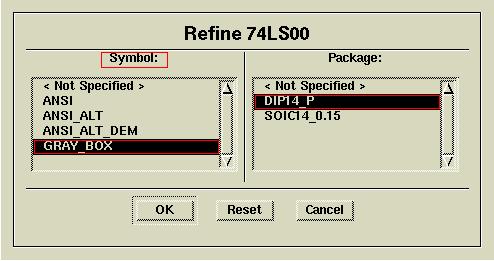
11) Select GRAY_BOX (the symbol for your schematic) and DIP14_P (the package) then click on OK. Click OK again in the Select Digital Logic Menu. You are now ready to place NAND gates on your design. Your screen should look like:
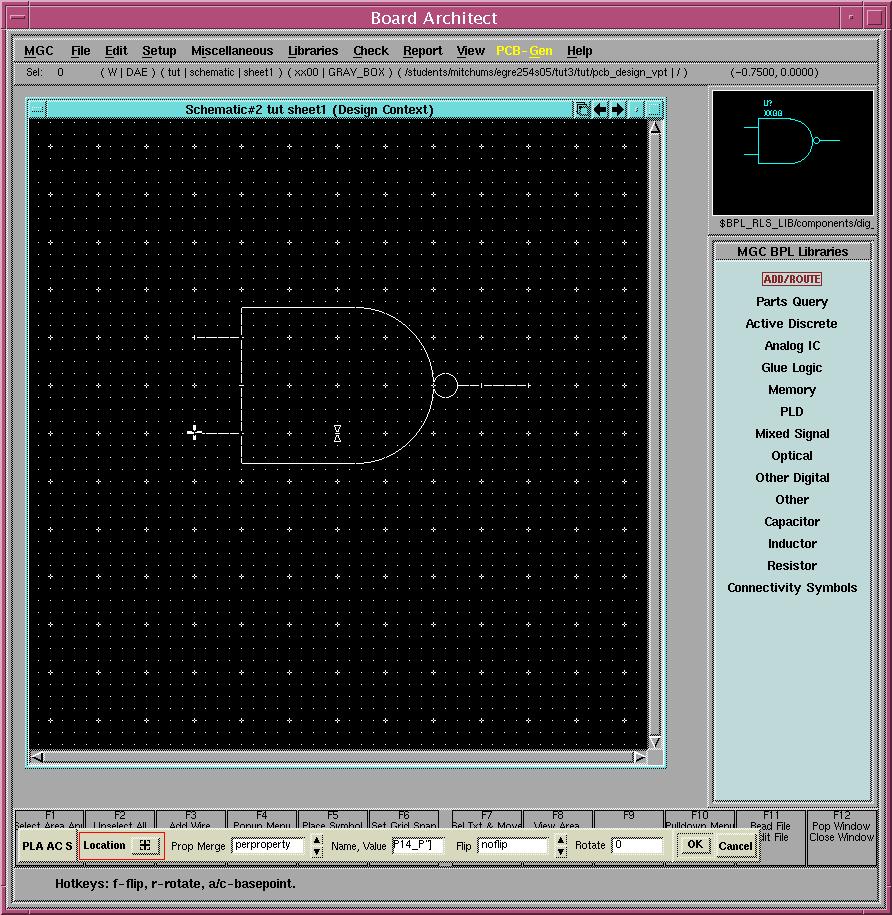
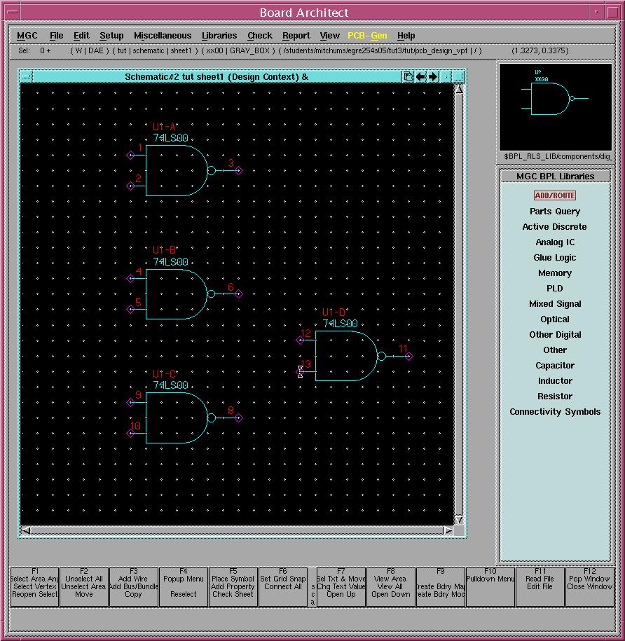
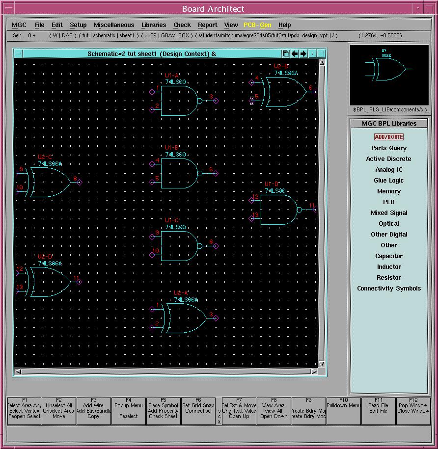
12) Place a NAND gate in the center of the screen by left clicking once. Then select View->Zoom Out->2.0. Now add a second NAND gate under the first NAND gate by clicking on the image of the NAND gate in the top left corner of the screen then clicking on the schematic page under the first NAND gate. Notice Board Architect has created reference numbers for your NAND gates (U1-A, U1-B) and given pin numbers for your NAND gates (1, 2 and 3 for the first NAND gate and 4, 5 and 6 for the second NAND gate). Board Architect is able to keep up with this information because you correctly selected the part, symbol and package from the library. Place two more NAND gates to make your screen look like:
13) Now repeat the same procedure as above to place 74LS86 XOR gates. First select Glue Logic in the schematic palette. You should see the Select Digital Logic popup menu:
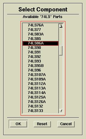
14) Select 74LS again for the Family. Then press the List Parts... button. You should see the Select Component dialogue box. Select 74LS86A as shown then select OK. (74LS86A is an improved version of the 74LS86 XOR gate) Your menu should look like:
15) Now press the Refine Component... button to pick the correct shape and footprint for the XOR gates. Again you should pick GRAY_BOX and DIP14_P as shown then select OK:
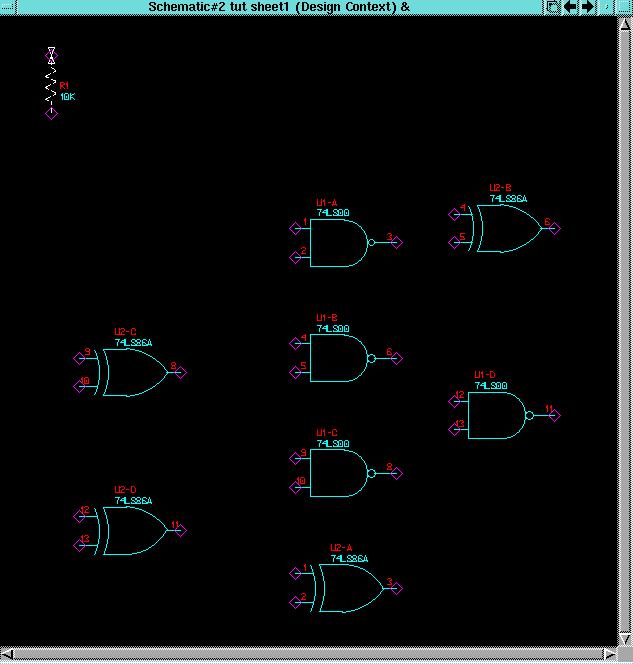
16) Now you are ready to add XOR gates to your schematic. Add four XOR gates to make your schematic look as shown:
17) Now you will add a pullup resistor. Sometimes it is necessary to use only one input of a gate and keep the other input at a high voltage. It is bad practice to leave inputs unconnected, though it is sometimes done with LS logic. It is also undesirable to connect a LS input directly to +5 Volts. So a resistor is used to limit current pulled by the input. 10K is a standard pullup for LS logic. To add a resistor, select Resistor from the schematic palette on the left. You will see the Select Resistor popup menu as shown:
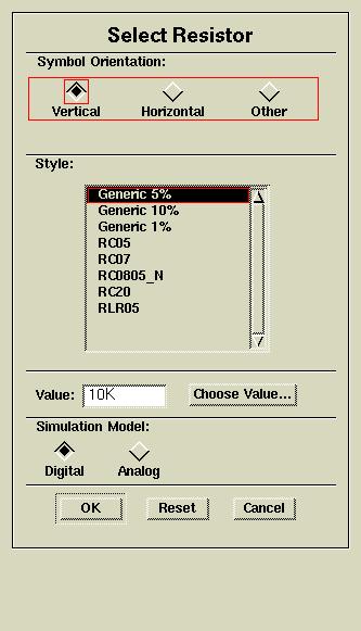
18) Select Generic 5% and enter the value 10K as shown. Make sure the Digital Simulation Model is selected. Then select OK. Place the resistor in the upper left of your schematic as shown:
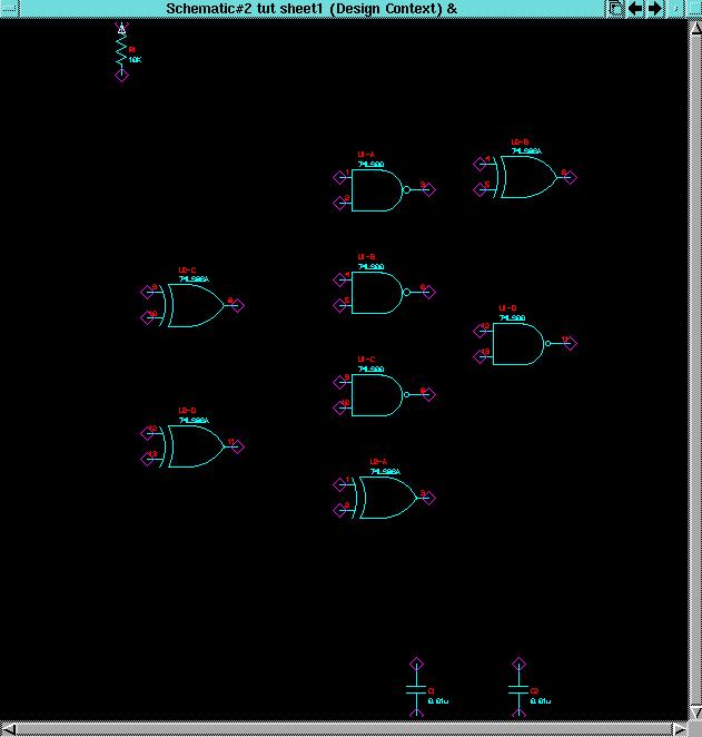
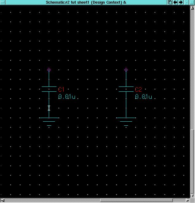
19) It is also very good practice to add capacitors across the power supply terminals of each IC. When a digital circuit switches, it creates a high current for a short amount of time. These switching currents generate a lot of noise in the power supply. Placing a capacitor across the power supply leads for each IC will filter a lot of this noise. You have two ICs (one quad NAND -U1- and one quad XOR -U2-) so you will need two capacitors. The location on the schematic is unimportant. Filter caps are typically shown at the bottom of the schematic page. When the circuit is built, however, they should be as close electrically as possible to the power supply pins for each IC. To place your two filter caps select Capacitor from the schematic palette on the left: You will see the Select Capacitor dialogue box:
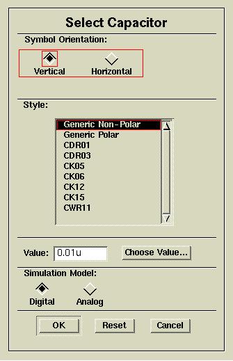
20) Select Generic Non-polar, Vertical, and Digital Simulation Model as shown. Then enter the value of 0.01u as shown. Then left click on the OK button. As with the other components, place the capacitors on your schematic as shown:
21) Now press F2 to deselect all components on your schematic. Then from the top menu select Libraries->Display Schematic Palette to display the schematic palette. Click once on the Add Wire icon to add wires to your schematic. Remember when adding wires, left click once to start a wire, left click once to add a wire segment and left click twice to terminate the wire. Add wires so your circuit looks like:
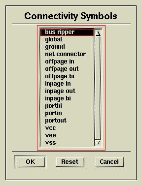
22) Now you need to add I/O connections. From the top tool bar select Libraries->MGC Board Process Libraries. From the side palette select Connectivity Symbols. You should see a popup menu with conectivity symbles:
23) Highlight ground and select OK. Place ground symbols on the bottom of the two capacitors. Remember you can use View->Area to zoom in to an area. Your capacitors should look like:
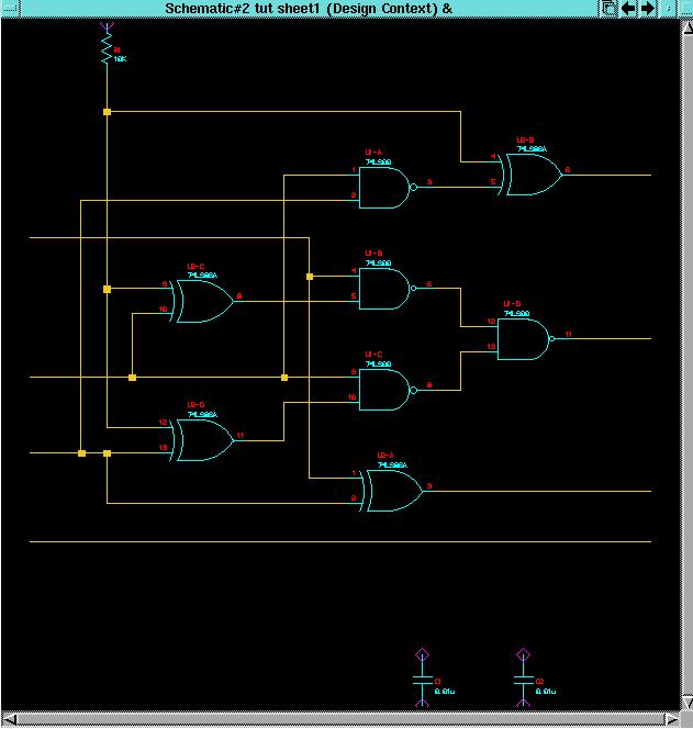
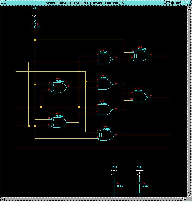
24) Now use the same procedure (Connectivity Symbols then choose Vcc) to add Vcc (+5 Volt) connections to the tops of the capacitors and the top of the resistor. Now your schematic should look like:
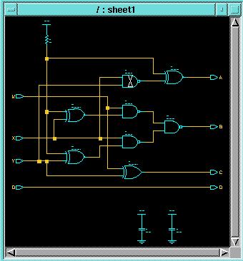
25) Now you need to add ports to your design to identify inputs and outputs for the simulator. Select Connectivity Symbols again then highlight portin and click OK to add input ports. First add one input port to the top left wire with no connection. Then place the cursor over the word NET and press both the Shift and the F7 keys at the same time. Enter W for the new net name then press Return. Now add another input port to the unconnected wire on the left. Change the name of this port to X. Add ports to the third and fourth and change the names of them to Y and Z, respectively. Your schematic should look like:
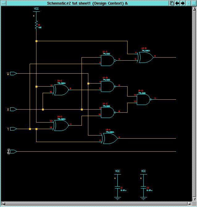
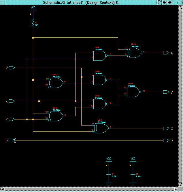
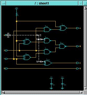
26) Now repeat the above process (click on Connectivity Symbols then highlight portout then click OK) to place output ports A, B, C and D. Note that once you name the output port D, Board Architect changes the name of the connected input port from Z to D. Board Architect will only allow a net to have one name. Your completed schematic should now look like:
27) From the top menu bar select Check->Sheet. You should have no errors or warnings in your schematic. Close the check report window. Now is also a good time to save the sheet (no errors) so select File->Save Sheet.
28) Now we will use Board Architect to create a net list.
A net represents a node in the schematic. For example, the connection
between U1-A pin 3 and U2-B pin 5 is a net. Board Architect keeps
up with all the nets in the circuit. Having Board Architect write
out the list of nets for you is a convenient way to make sure you know
how to wire this circuit. Select File->Save PCB->nets As to
generate a netlist. You will see another popup menu asking for the
name of the file where you want the net list written as shown:
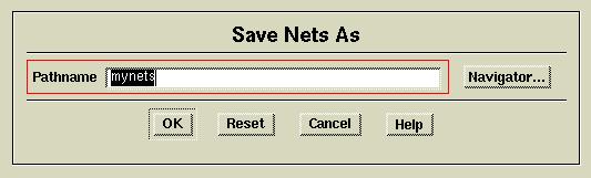
29) Type in mynets into the Pathname location and click on OK. This will cause Board Architect to write the netlist into the file called mynets at the current directory. Now you can use a text editor to view the file and print it. Move to the bottom control panel on the screen and left click once on the small arrow above the notecard:

30) You should see a popup menu as shown:
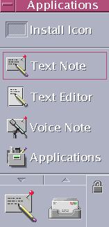
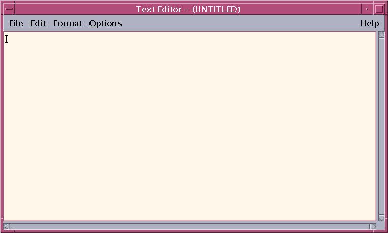
31) Left click once on the Text Editor item to open a text editor as shown below:
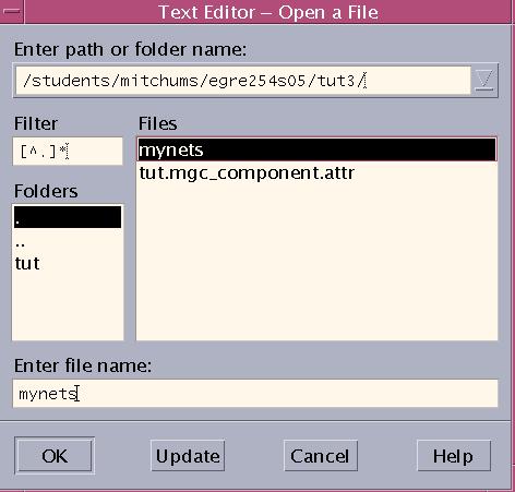
32) Inside the text editor choose File->Open. You will see the open dialogue box. Navigate to the directory containing your design, tut3. Then select the file mynets. Your dialogue box should look similar to this:
33) Click OK to open the net list. Your text editor display should look something like this:
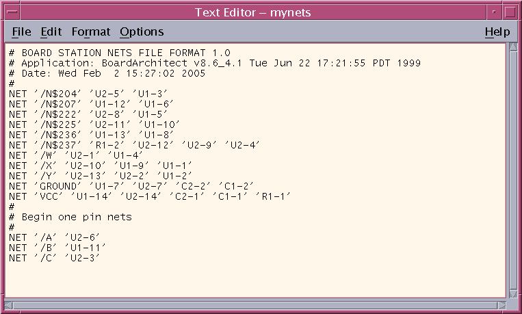
34) Notice each set of connections is called out in a NET statement. The format is: NET 'netname' 'chip-pin' 'chip-pin' etc. You can use this net list to wire the circuit. From the net list you can see that you need to connect a wire from U2-5 to U1-3, for example. Notice also Board Architect is telling you to connect Vcc (+5 Volts) to pin 14 of each IC (U1-14, U2-14) and to the tops of the capacitors and resistor (C2-1, C1-1, R1-1). Using a wire list to check your prototyping can save you a lot of time in lab.
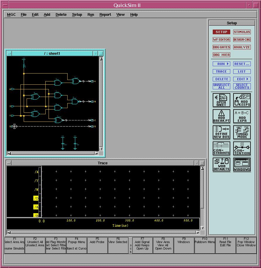
35) You can print the netlist and take it into the 254 lab to help you wire the circuit. Choose File->Print from the text editor menu bar. You will see a print dialogue box like this:
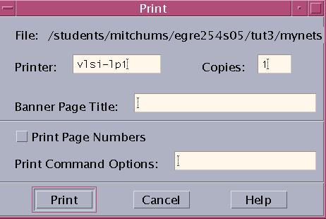
36) You do not need to change anything. Just click on the PRINT button. Close the text editor by selecting File->Close.
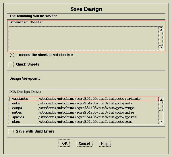
38) The defaults are fine. Left click once on OK to save your design. Note that saving will also run a check on the schematic sheet.
39) After the design has been saved, close the check report. Then close Build Architect by selecting MGC->Exit from the top menu.
41) Click the Navigator button to see the following menu:
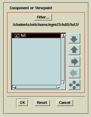
42) Highlight the component (tut) and click OK on the Component or Viewpoint menu. Then click OK on the Set Viewpoint menu. You will get the Open Design Sheet menu as before:
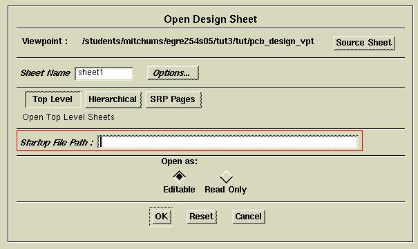
43) Click OK to open your existing design. Remember
to use File->Save PCB->All to save any work you do on your design.
After you have finished altering your design and saving it, close Board
Architect.
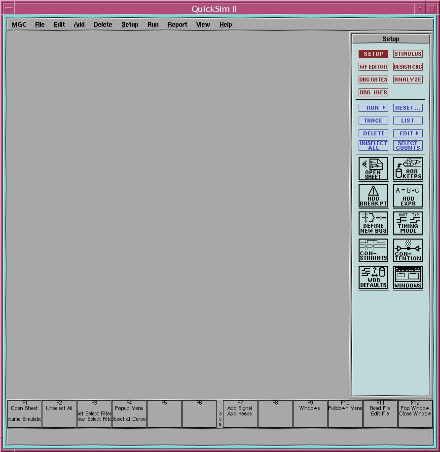
45) Now you can start Quicksim as you did in tutorial 1 by typing the following command line: quicksim -tim typ tut & then press the Return key.
![]()
46) You should see the opening screen for Quicksim as shown:
47) Use the Open Sheet icon or File->Open Sheet to open your schematic. You will get a small window containing your schematic as shown:
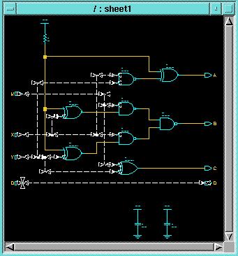
48) As before, you need to tell Quicksim what signals to trace. Make sure the schematic window is highlighted (the border is torquise - not gray) then use the mouse to select signals X, Y, Z and D. You may left click once on each signal to select it or you may draw a box around one or more signals to select them. Selected signals appear dashed as shown below:
49) Once you have selected all four input signals, add them to
the trace list by either clicking once on the TRACE palette item ![]() or by right clicking once inside the schematic window then selecting Add->Traces
from the popup menu. Now highlight the schematic window again by
left clicking once on the top bar then press F2 to deselect the
input signals. Select the four output signals and add them to the
trace as you did the input signals. Now your Quicksim window should
look like:
or by right clicking once inside the schematic window then selecting Add->Traces
from the popup menu. Now highlight the schematic window again by
left clicking once on the top bar then press F2 to deselect the
input signals. Select the four output signals and add them to the
trace as you did the input signals. Now your Quicksim window should
look like:
50) You can move the schematic window up and resize the trace window so that all signals will show. Now you must assign forces to the inputs. First make sure the schematic window is highlighted. Then press the F2 key on the keyboard to deselect everything. Now you will add a force to signal W. (A force is how you describe an input signal to the simulator.) Select signal W by either left clicking on the signal or holding the left mouse button down and drawing a box containing only signal W. Your schematic box should look like:
51) As in tutorial 1, you will add a multiple value force. Right click once inside the schematic window. Then right click once on the small arrow to the right of the popup menu item Force. You should see the following:
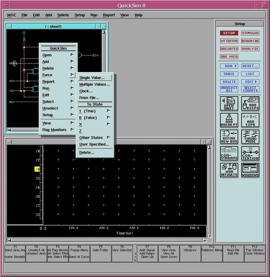
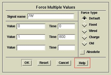
52) Now select Multiple Values... from the second popup menu. You will get a dialogue box that looks like:
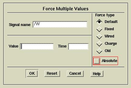
53) Fill in the dialogue box with the values 0, 0, 1, 800 as shown:
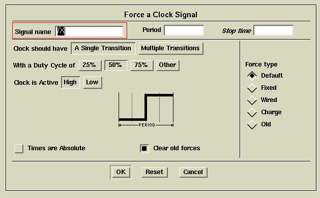
54) When you have entered all the forces, press the Return key to complete this dialogue box. You still need to provide an input signal for X, Y and D. So press F2 on the keyboard to deselect W. There is an easier way to define forces for many instances. Instead of using Force Multiple Values, you can setup each force as a clock. You will setup signals X, Y and Z as clocks. First make sure the schematic window is highlighted. Then press F2 to deselect signal W. Then select signal X. Now right click once in the window, then once on the arrow beside Force as before. But this time select Clock from the Force popup menu. You will see the Force a Clock Signal dialogue box as shown:
55) Fill out the dialogue box as shown (you only need to make the period 800)then click OK:
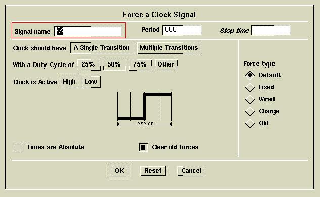
56) Add a clock force to Y with a period of 400 and a clock force to D (Z) with a period of 200. Notice the pattern. You set W low 800 and high 800 seconds (period = 1600). Then you set X period to 800. Then you set Y period to 400. Finally you set Z (D) period to 200. So each signal is half the previous one. This pattern will give all possible input values for the four inputs.
57) Now you are ready to run the simulation. From the top Quicksim menu select Run->For Time. You will get a small dialogue box at the bottom of your screen like this:
![]()
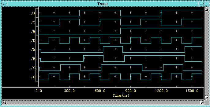
58) Enter 1600 for the time (one period of the slowest input signal) then click OK. You should get a simulation trace similar to the one shown here:
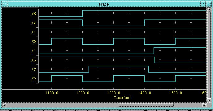
59) You can use the View->All command to expand the trace to the entire window. Your completed, expanded trace should look like:
60) You can print the trace, as in Tutorial 1, by first highlighting the trace window then selecting File->Print->Active Window. You will see the Print Traces dialogue box. Enter mgcprint for the printer name as shown:
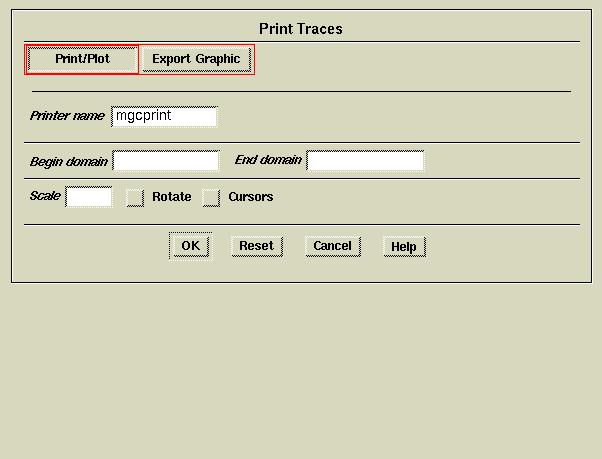
61) Then select OK to print the trace. Being able to simulate a prototype before you build it is very powerful. You can take the printout of the simulation to lab and compare it to your prototyped circuit. Close the simulator by selecting MGC->Exit from the top menu. Select Without Saving in the Exit Quicksim dialogue box as shown:
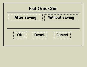
62) Select OK to terminate Quicksim.