2) In general, create a separate directory for each design you make. In this case, use a Console or Terminal to create a new directory for this tutorial then change your working directory to this new directory and startup Board Architect:
vlsi01> mkdir tut3
vlsi01> cd tut3
vlsi01> ba &
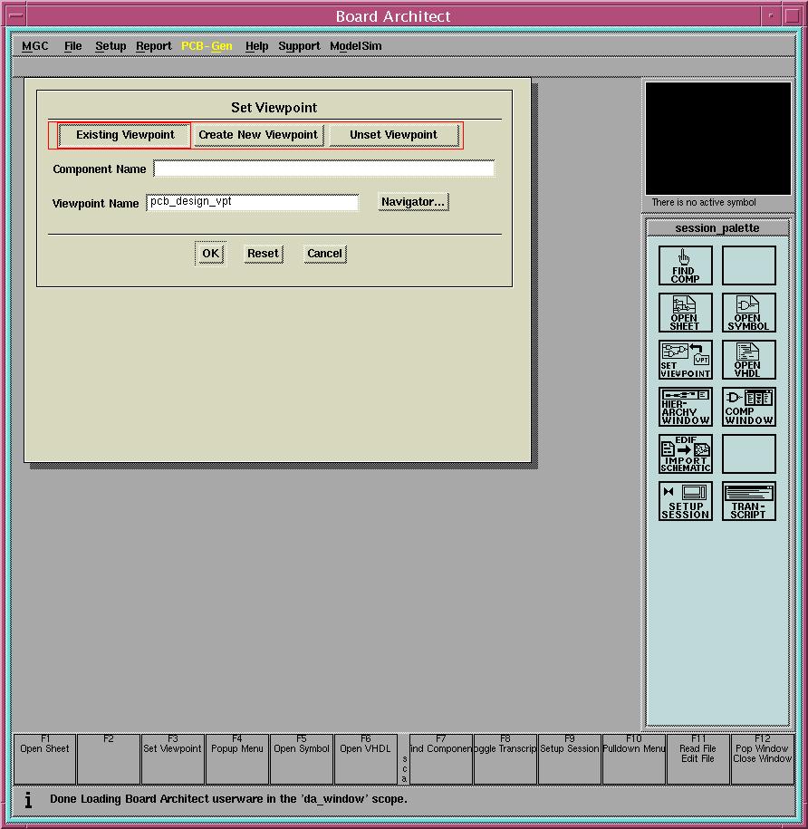
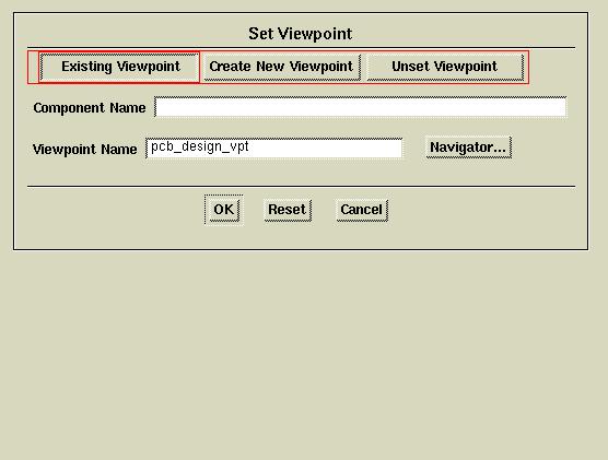
3) Use the File->Open->Set Viewpoint command (or the Set Viewpoint icon on the menu) to create a new viewpoint into your design. Your screen should look like this:
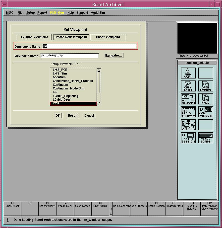
4) You want to create a new viewpoint for your design (a viewpoint is the portal through which the Mentor software sees your design). Type in tut for the name of the design and select PCB for the type of viewpoint. Your screen should look like:
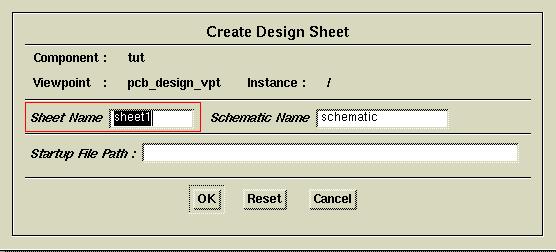
4) Select OK. Next you will see another popup window for creating the first sheet in your design. Leave the Sheet Name as sheet1. Select OK in this window as well.
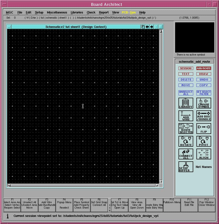
5) Your screen should now show a blank schematic page and
the default library palette like this:
6) To get 74LS logic parts, we need to open the appropriate library. Left click once on Libraries in the top menu bar. Then left click once on MGC Board Process Libraries in the pull down menu. Your screen should now look like:

7) Now to get the 74LS parts, select Glue Logic. You will get a menu of available digital part families. The menu should look like:
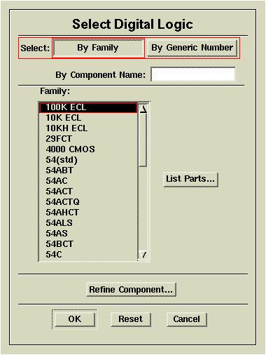
8) From within this menu select 74LS in the scrolling window. Then click once on the List Parts button. You will see a new menu listing all the 74LS parts in the system:
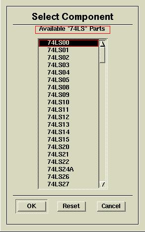
9) Highlight 74LS00 (NAND gates) and then click OK once to return to the Select Digital Logic menu. Then click the Refine Component... button to define the package and symbols. You should see another menu as shown:
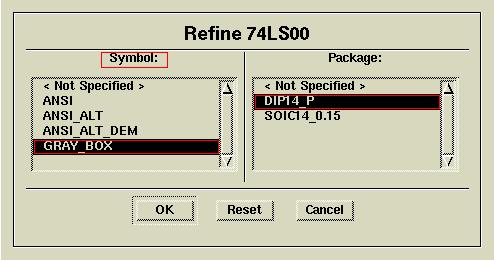
10) Select GRAY_BOX (the symbol for your schematic) and DIP14_P (the package) then click on OK. Click OK again in the Select Digital Logic Menu. You are now ready to place NAND gates on your design. Your screen should look like:
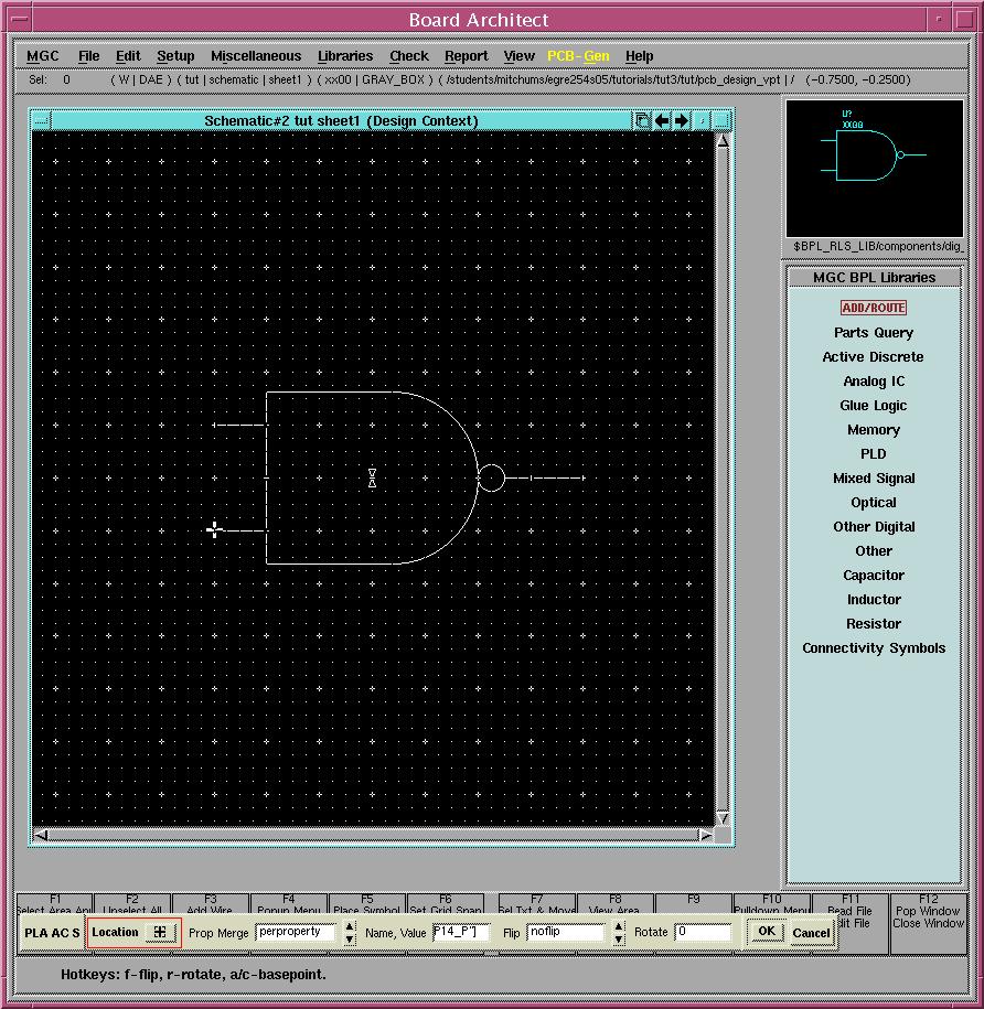
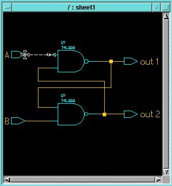
11) Place a NAND gate in the center of the screen by left clicking once. Then select View->Zoom Out->2.0. Now add a second NAND gate under the first NAND gate by clicking on the image of the NAND gate in the top left corner of the screen then clicking on the schematic page under the first NAND gate. Notice Board Architect has created reference numbers for your NAND gates (U1-A, U1-B) and given pin numbers for your NAND gates (1, 2 and 3 for the first NAND gate and 4, 5 and 6 for the second NAND gate). Board Architect is able to keep up with this information because you correctly selected the part, symbol and package from the library. Your screen should now look like:

12) Now press F2 to deselect the two NAND gates. Then from the top menu select Libraries->Display Schematic Palette to display the schematic palette. Click once on the Add Wire icon and add wires to make your schematic match the screen below (cross coupled NAND gates make a flip-flop).
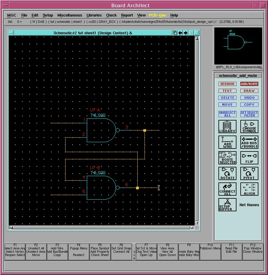
13) Now you need to add I/O connections. From the top tool bar select Libraries->MGC Board Process Libraries. From the side palette select Connectivity Symbols. You should see a popup menu with conection symbles:
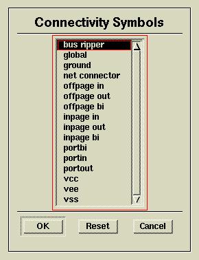
14) Highlight portin and click OK to add input ports. First add one input port to the top NAND gate. Then place the cursor over the word NET and press both the Shift and the F7 keys at the same time. Enter A for the new net name then press Return. Now add another input port to the lower NAND gate. Change the name of this port to B. Your screen should look like:
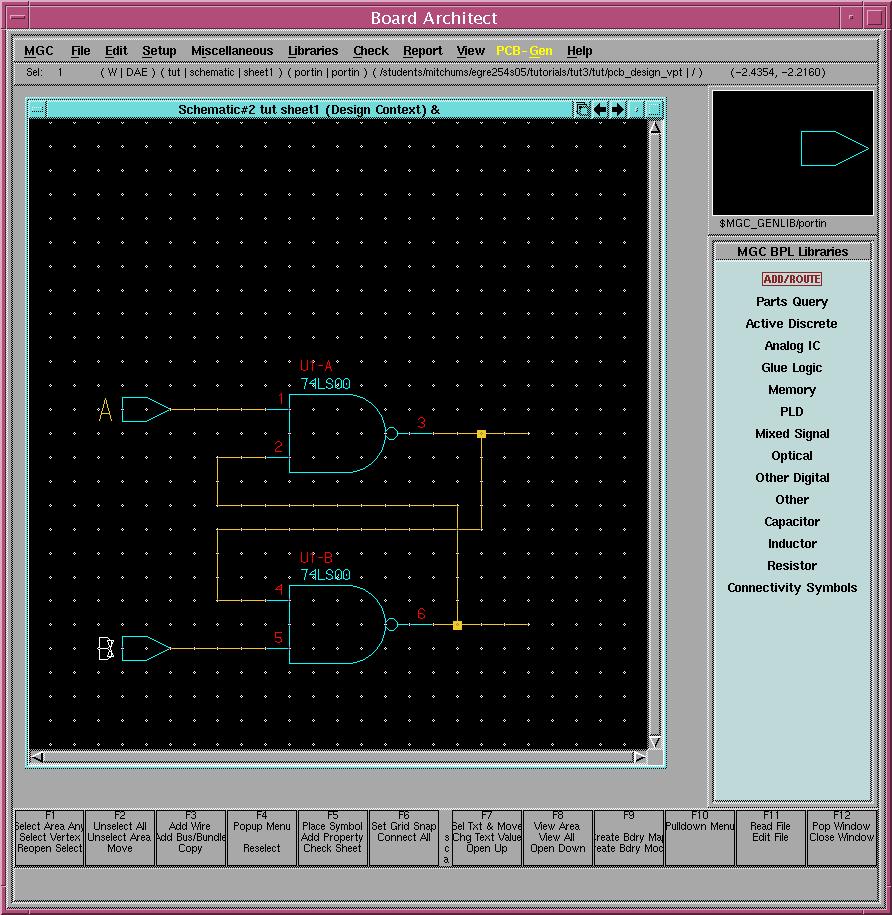
15) Now repeat the above process (click on Connectivity Symbols then highlight portout then click OK) to place output ports out1 and out2. Remember you cannot use spaces in the names out1 and out2. Your screen should now look like:
16) From the top menu bar select Check->Sheet. You
should have no errors or warnings in your schematic. Close the check
report window.
17) Now we will use Board Architect to create a net list.
A net represents a node in the schematic. For example, the connection
between pin 3 and pin 4 is a net. Board Architect keeps up with all
the nets in the circuit. Having Board Architect write out the list
of nets for us is a convenient way to make sure we know how to wire this
circuit. Select File->Save PCB->nets As to generate a netlist.
You will see another popup menu asking for the name of the file where you
want the net list written as shown:
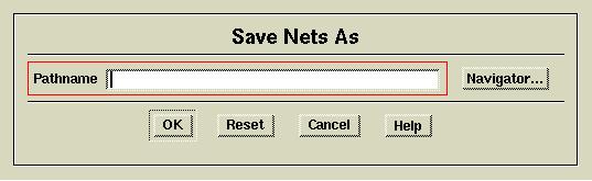
18) Type in mynets into the Pathname location and click on OK. This will cause Board Architect to write the netlist into the file called mynets at the current directory. Now you can use a text editor to view the file and print it. Move to the bottom control panel on the screen and left click once on the small arrow above the notecard:

19) You should see a popup menu as shown:
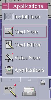
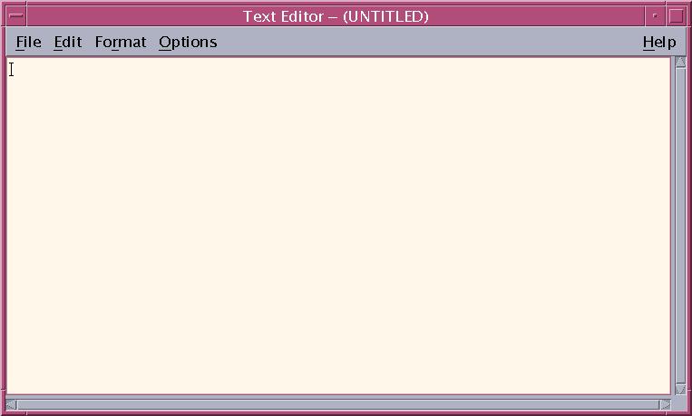
20) Click once on the Text Editor item to open a text editor as shown below:
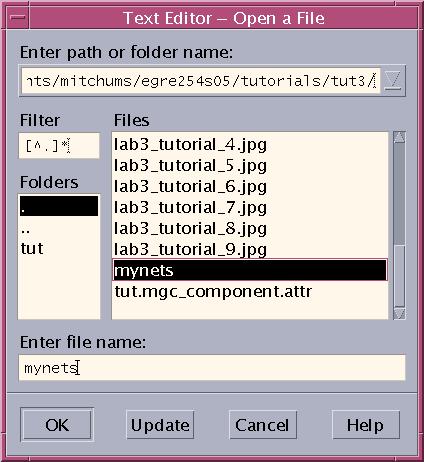
21) Inside the text editor choose File->Open. You will see the open dialogue box. Navigate to the directory containing your design, tut3. Then select the file mynets. Your dialogue box should look similar to this:
22) Click OK to open the net list. Your text editor display should look something like this:
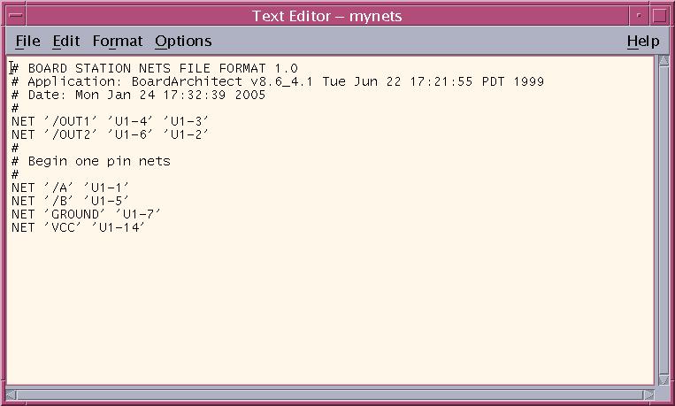
23) Notice each set of connections is called out in a NET statement. The format is: NET 'netname' 'chip-pin' 'chip-pin' etc. You can use this net list to wire the circuit. From the net list you need to connect pins 3 and 4 together with a wire, connect pins 2 and 6 together with a wire, connect GROUND to pin 7 and connect +5V (VCC) to pin 14. You also see your input A should be connected to pin 1 and B should be connected to pin 5.
24) You can print the netlist and take it into the 254 lab to help you wire the circuit. Choose File->Print from the text editor menu bar. You will see a print dialogue box like this:
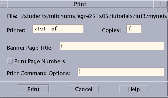
25) You do not need to change anything. Just click on the PRINT button.
26) Close the text editor by selecting File->Close.
27) Save your tutorial schematic by selecting File->Save
PCB->All. This will bring up a Save Design window:
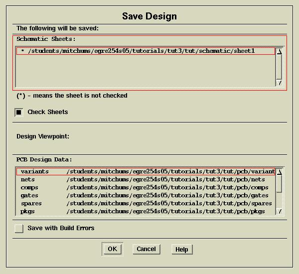
28) The defaults are fine. Left click once on OK to save your design. Note that saving will also run a check on the schematic sheet.
29) After the design has been saved, close the check report.
Then close Build Architect by selecting MGC->Exit from the top menu.
31) Click the Navigator button to see the following menu:
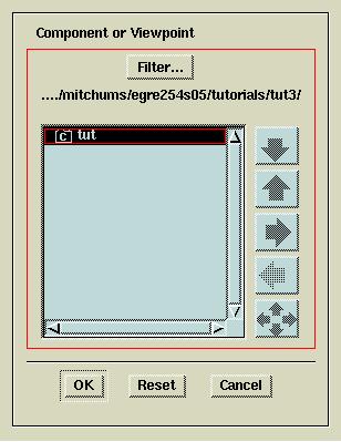
32) Highlight the component (tut) and click OK on the Component or Viewpoint menu. Then click OK on the Set Viewpoint menu. You will get the Open Design Sheet menu as before:
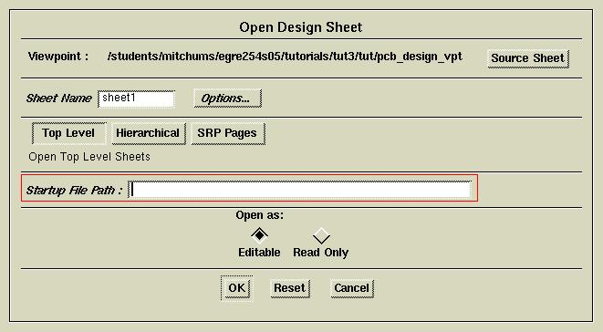
33) Click OK to open your existing design. Remember
to use File->Save PCB->All to save any work you do on your design.
After you have finished altering your design and saving it, close Board
Architect.
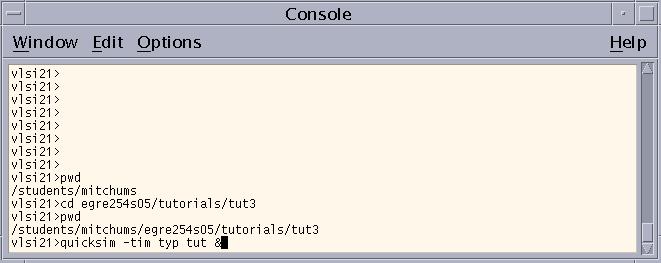
35) Now you can start Quicksim as you did in tutorial 1 by typing the following command line: quicksim -tim typ tut & then press the Return key.
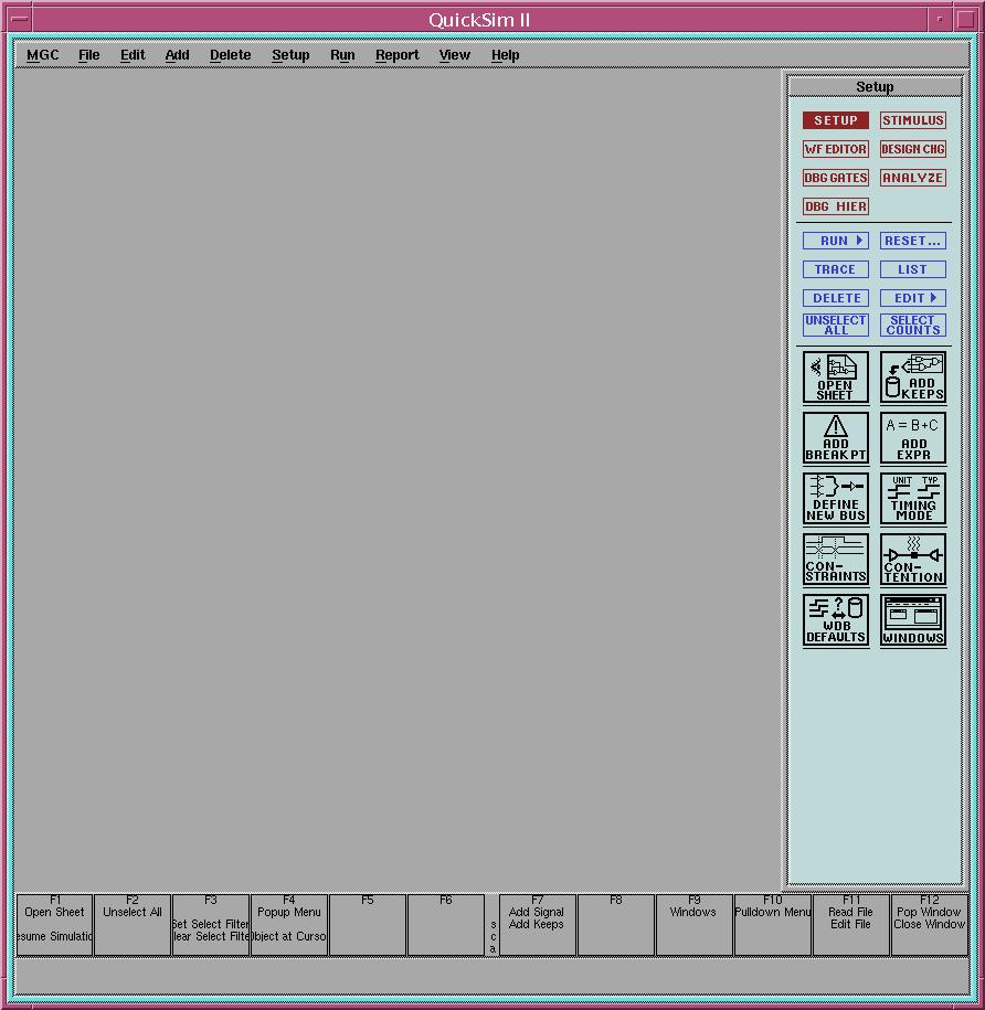
36) You should see the opening screen for Quicksim as shown:
37) Use the Open Sheet icon or File->Open Sheet to open your schematic. You will get a small window containing your schematic as shown:
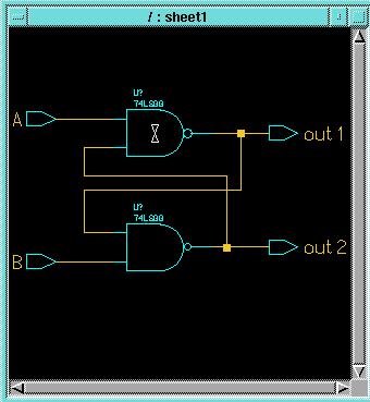
38) As before, you need to tell Quicksim what signals to trace. Make sure the schematic window is highlighted (the border is torquise - not gray) then use the mouse to select signals A, B, out1 and out2. You may left click once on each signal to select it or you may draw a box around one or more signals to select them. Selected signals appear dashed as shown below:
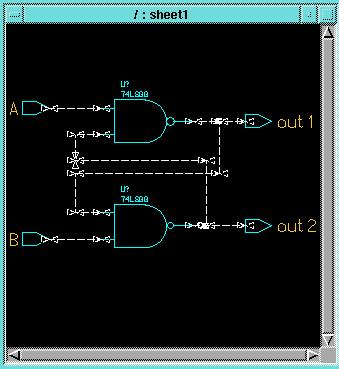
39) Once you have selected all four signals, add them to the trace
list by either clicking once on the TRACE palette item ![]() or by right clicking once inside the schematic window then selecting Add->Traces
from the popup menu. Now your Quicksim window should look like:
or by right clicking once inside the schematic window then selecting Add->Traces
from the popup menu. Now your Quicksim window should look like:
40) Now you must assign forces to the inputs. First make sure the schematic window is highlighted. Then press the F2 key on the keyboard to deselect everything. Now you will add a force to signal A. (A force is how you describe an input signal to the simulator.) Select signal A by either left clicking on the signal or holding the left mouse button down and drawing a box containing only signal A. Your schematic box should look like:
41) As in tutorial 1, you will add a multiple value force. Right click once inside the schematic window. Then right click once on the small arrow to the right of the popup menu item Force. You should see the following:
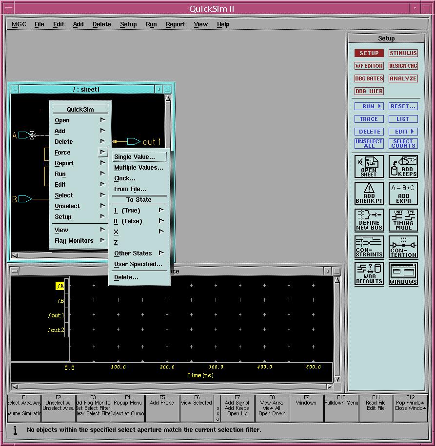
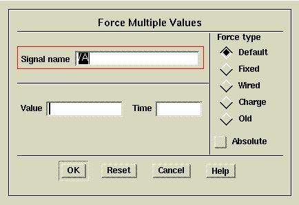
42) Now select Multiple Values... from the second popup menu. You will get a dialogue box that looks like:
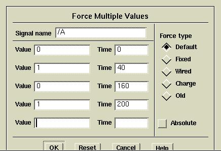
43) Fill in the dialogue box with the values 0, 0, 1, 40, 0, 160, 1, 200, as shown:
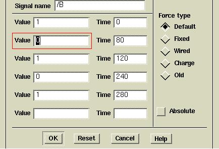
45) When you have entered all the forces, press the Return key to complete this dialogue box. You still need to provide an input signal for B. So press F2 on the keyboard to deselect A then select signal B. Repeat the procedure to obtain the Force Multiple Values dialogue box for B. Then enter 1, 0, 0, 80, 1, 120, 0 240, 1, 280 as shown:
46) Select OK or press the Return key to complete signal B setup. Now you are ready to run the simulation. From the top Quicksim menu select Run->For Time. You will get a small dialogue box at the bottom of your screen like this:
![]()
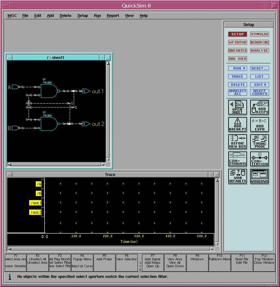
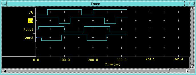
47) Enter 320 for the time as shown then click OK. You should get a simulation trace similar to the one shown here:
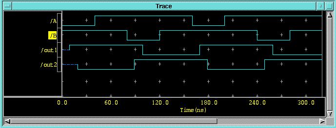
48) You can use the View->All command to expand the trace to the entire window. Your completed, expanded trace should look like:
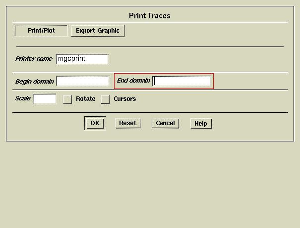
49) You can print the trace, as in Tutorial 1, by first highlighting the trace window then selecting File->Print->Active Window. You will see the Print Traces dialogue box. Enter mgcprint for the printer name as shown:
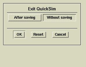
50) Then select OK to print the trace. Close the simulator by selecting MGC->Exit from the top menu. Select Without Saving in the Exit Quicksim dialogue box as shown:
51) Select OK to terminate Quicksim.