1) Selection: Whenever you want to MOVE, COPY, DELETE or CHANGE PROPERTIES you need to select the thing(s) you want to work on. A selected item appears as dashed white in a schematic. Once you have the item(s) selected then you can just press the DEL key to delete it. You can right-click to get a local menu of things you can do with the selected item(s) such as moving it. You can select multiple items (wires, components, etc.) and move them all at once (or delete them all at once - hence be careful). You can select by:
3) The ESC key is used to terminate (escape) from commands. For instance, when adding wires you will notice a small brown dialogue box on the screen. When you are through adding wires, press the ESC key and the box will disappear. Also if you are navigating menu selections from the top bar menu and you want to quit without taking any action then press the ESC key.
4) Adding components: Usually you have to navigate to where the component image is store in Board Architect or Design Architect. Normally you have to get to the right library (easiest way is to use the Libraries entry in the top menu bar) then get to the correct parts grouping (easiest way is to pick from a list on the right hand side menu) then pick the specific component you wish to place.
5) Adding wires: You must return to the Default Schematic Pallete to add wires to your design. As with adding components, use the Libraries entry in the top bar menu.
6) Changing text on your schematic: Changing text is such a common function that Board Architect has a very handy shortcut for doing it. Use the mouse to lay the cursor arrow over the top of the word(s) you want to change (without clicking the mouse) then press both the SHIFT and F7 keys at the same time. You get a small dialogue box with the name highlighted in it. Type in the new name followed by a RETURN.
7) Zoom in and out: No matter what else you are doing, you can always zoom in and out. Board Architect has several handy ways to do this:
9) Board Architect keeps a lot of information about
your design in various databases. For example, there is a schematic
database containing the components that make up the schematic, a simulation
database containing the information for simulating the components, a PCB
database with information required to make a printed circuit board and
others. Whenever you see the word viewpoint in a Mentor tool that
usually refers to a specific database for your design. You will be
working with the PCB viewpoint in this tutorial as you want both the circuit
and the physical information like pin and package numbers.
2) The equations:
4) You will learn how to add a pullup resistor on the reset (CLR) pin for the flipflops and simulate the pullup resistor properly. Flipflops are a little harder because the Quicksim simulator must know an initial condition of the flipflops in order to solve the circuit. So you MUST supply a reset of some type for the flipflops. This tutorial shows one method.
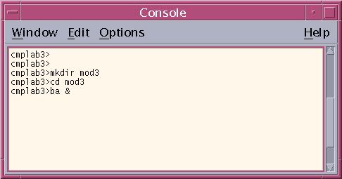
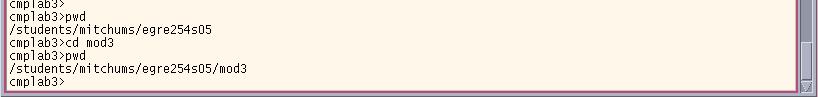
2) In general, create a separate directory for each design you make. Create the directory using the mkdir command then change your working directory to this new directory using the cd command then startup Board Architect:
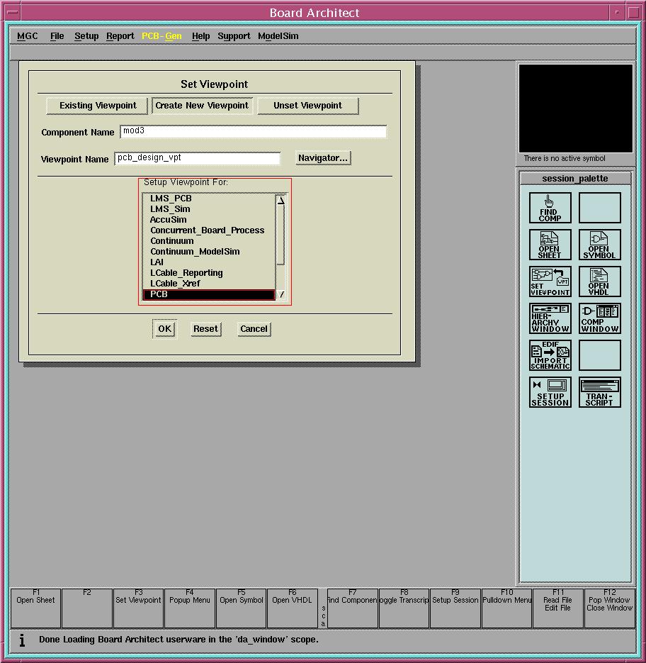
3) From the top menu bar in BA, use the File->Open->Set Viewpoint command (or the Set Viewpoint icon on the menu) to create a new viewpoint into your design. You will create a new Viewpoint. (Each design has one or more viewpoints in the Mentor tools. A particular viewpoint controls how the Mentor tools interact with your design. Choosing the PCB viewpoint prepares BA to create a real circuit with real ICs, real timing information, real parts and real pin numbers). Fill in the dialogue box as shown below:
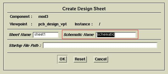
4) Select OK. Next you will see another popup window for creating the first sheet in your design. Leave the Sheet Name as sheet1 and the Schematic Name as schematic. Select OK in this window as well.
5) Board Architect is very similar to Design
Architect - you would use Design Architect if you will implement your design
in an ASIC or FPGA but you would use Board Architect if you will prototype
your design using logic chips or your will implement your design as a PCB.
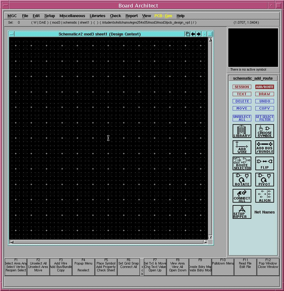
Your screen should now show a blank schematic page as below. Grab
a corner of the Board Architect window, hold the left mouse button down
and drag the corner to make the screen as large as you want. This
tutorial uses a screen size of 900 x 900 pixels. Use a bigger screen
to be able to see more circuit area. Don't worry if the grid inside
your schematic sheet looks different than the one below. BA will
change the grid based on how much you are zoomed in or out. Your
screen should look similar to the one below:
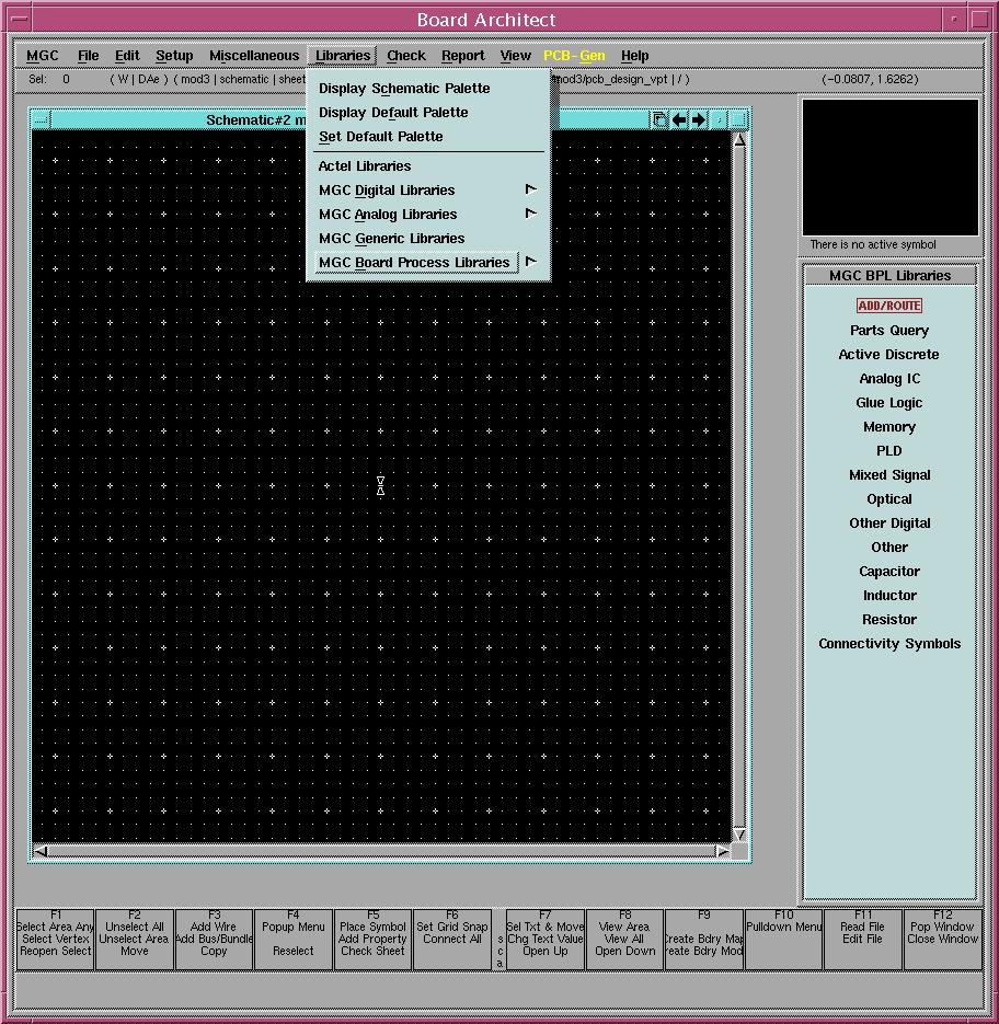
6) To get 74LS logic parts, you need to open the appropriate library. Left click once on Libraries in the top menu bar. Then left click once on MGC Board Process Libraries in the pull down menu. Your screen should now look like:
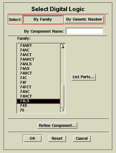
7) The first thing you want to do is place the flipflops and XOR gates on your schematic. To get the 74LS parts, select Glue Logic from the right hand menu. All the standard logic parts like inverters, nand gates, nor gates and flipflops are considered glue logic by Board Architect. You will get a list of available digital part families. Use the scroll bar to select the 74LS family of parts. The dialogue box should look like:
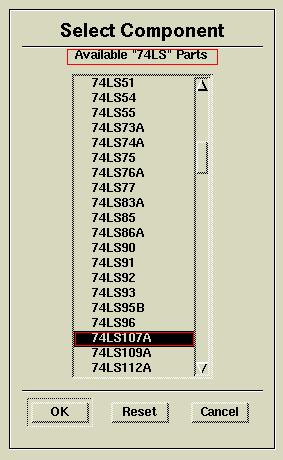
8) From within this list select 74LS in the scrolling window. Then click once on the List Parts button. You will see a new dialogue box listing all the 74LS parts in the system. Use the scroll bar to select 74LS107A, the J-K flipflops you need for your design. The dialogue box should look like:
9) Highlight 74LS107A (J-K flipflops) and then click OK once to return to the Select Digital Logic menu. Then click the Refine Component... button to define the package and symbols. This is how you pick a particular package and pin configuration of 74LS107A's. You must use Refine Component if you want Board Architect to assign pin numbers and chip numbers for you. You should see another dialogue box as shown:
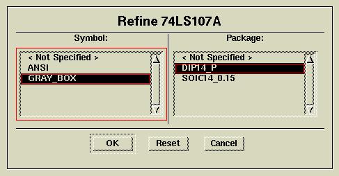
10) Select GRAY_BOX (the symbol for your schematic) and DIP14_P (the package) then click on OK. Click OK again in the Select Digital Logic Dialogue Box. You are now ready to place J-K flipflops on your design. Your screen should look like:
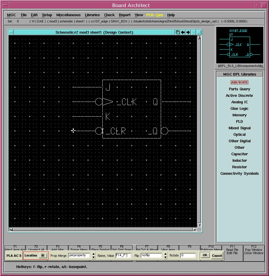
11) Place a flipflop in the center of the screen by left clicking once. Then from the top menu bar select View->Zoom Out->2.0. Now add another flipflop by left-clicking on the image of the flipflop in the top right corner of the screen then clicking on the schematic page where you want to place the flipflops. Notice Board Architect has created reference numbers for your flipflops (U1-A, U1-B) and given pin numbers for your flipflops. Board Architect is able to keep up with this information because you correctly selected the part, symbol and package from the library. Your J-K flipflops are dashed because they are currently selected. Press F2 to unselect everything on the schematic. (Remember F2 always unselects everything. Use it often to keep from accidentally deleting objects from your schematic.) Your screen should look like:
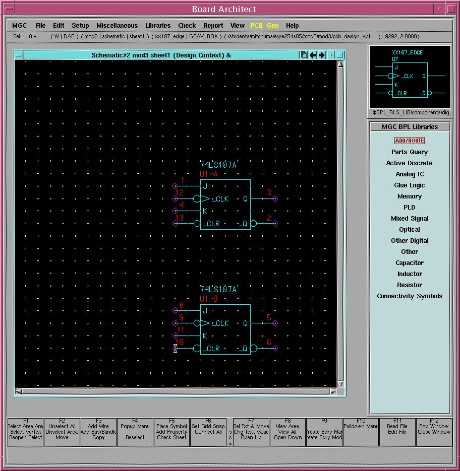
12) Now repeat the same procedure as above to place two (2) 74LS86A XOR gates. Remember to select the Refine Components button and select GRAY_BOX and DIP14_P. Here are some tips: The blue square in the top right corner of the schematic sheet will expand the schematic to fill the available area. You can use the View->Zoom-> commands at any time to zoom in and out of your drawing. You can use the scrolling bars on the right and bottom of the schematic page to scroll the schematic. Even if a scrolling bar appears to be all the way up or down, you can still use it to show you more "blank page" for working. After you place the XOR gates, press F2 to deselct all. Now your screen should look like:

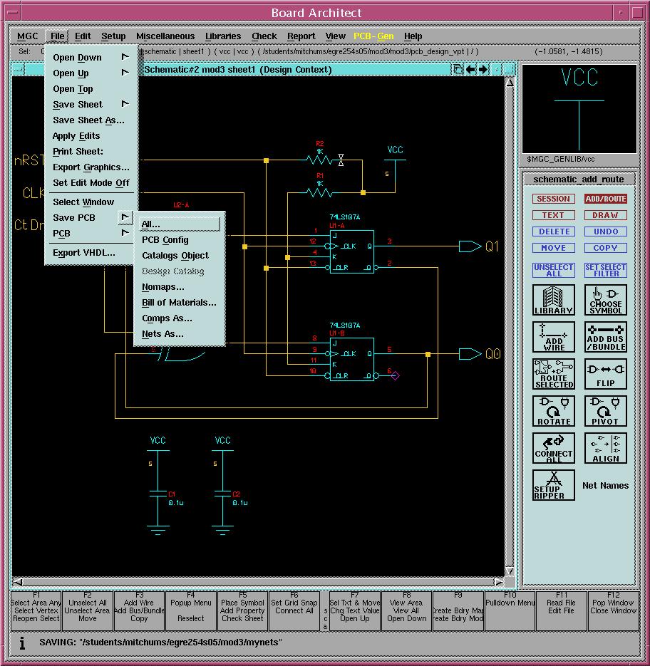
13) Now is a good time to add some wires to the schematic. From the top menu select Libraries->Display Schematic Palette to display the schematic palette. Left-click once on the Add Wire icon to add wires to your schematic. Here are some tips for adding wires. Left-click once to start a wire. Left-click once every time you want to change direction (like horizontal to vertical). Left-click twice to terminate the wire. Press ESC when you want to stop adding wire. Remember to use F2 to deselect all before selecting and deleting a wire. To delete a wire: First press F2 to deselect everything and ESC to stop adding wires. Then left-click once on the wire you want to delete. It should turn from solid to dashed - showing it is selected. Then press the DEL key. Add wires so your circuit looks like:
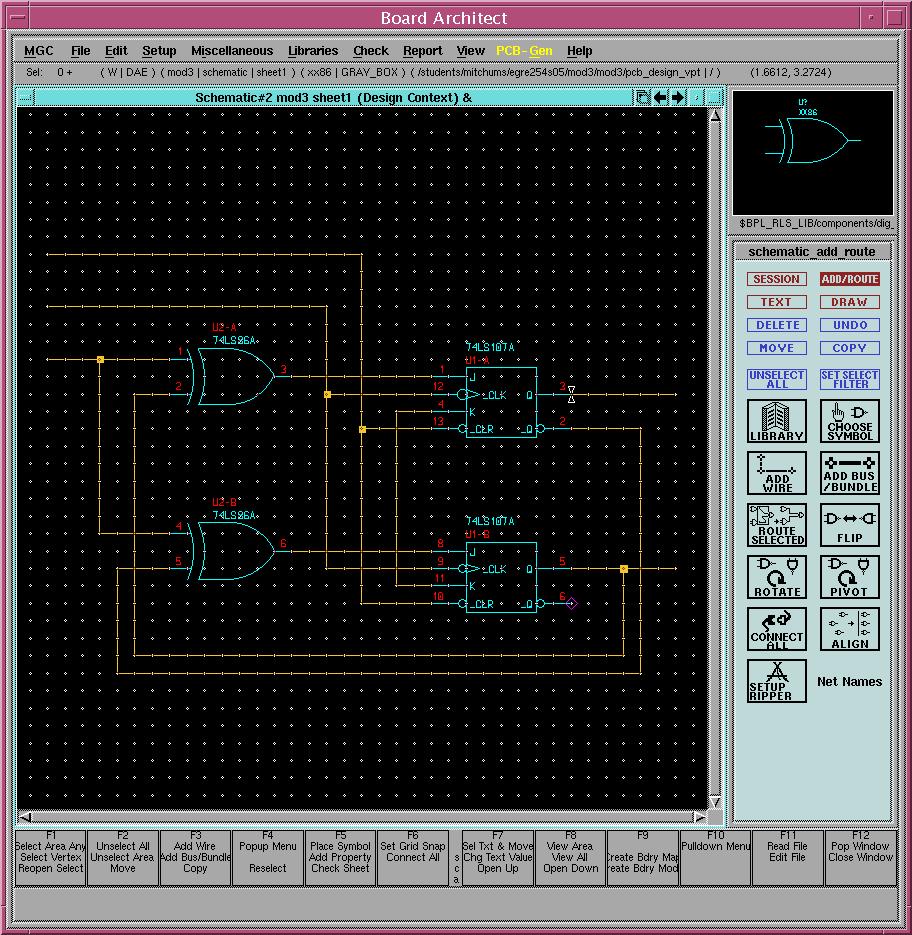
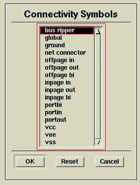
14) Now you can add the ports (inputs and outputs) to the schematic. We have to switch back to the MGC Board Process Libraries for these as they are specific to the PCB (printed circuit board) viewpoint. From the top menu bar select Libraries->MGC Board Process Libraries as before. This time, instead of Glue Logic (where the 'LS parts are) select Connectivity Symbols from the right side menu. You will get a dialogue box that lists the available connections. Note GROUND and VCC are here as well - you will need them later. The dialogue box should look like:
15) You are going to place input and output ports and name them. Place one port at a time and change the name of it from NET to the correct name for your design. First you will place and name the output ports, Q1 and Q0. From this dialogue box select the portout entry and press OK. It will look like you are placing a gate or flipflop but now you are placing an output port. Put the cursor just at the end of the wire coming out of the Q pin on the top flipflop and left-click. The port should be attached to the wire as shown below:
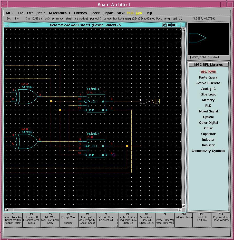
16) Now, before placing any more ports, you will change the name of this port from NET to Q1. First position the red cursor exactly on top of (over it - not above it) the word NET by the output port. DO NOT CLICK. While the cursor is over the word NET, press the Shift and the F7 keys at the same time. You will see a small dialogue box at the bottom of your schematic and the word NET will be highlighted as shown:
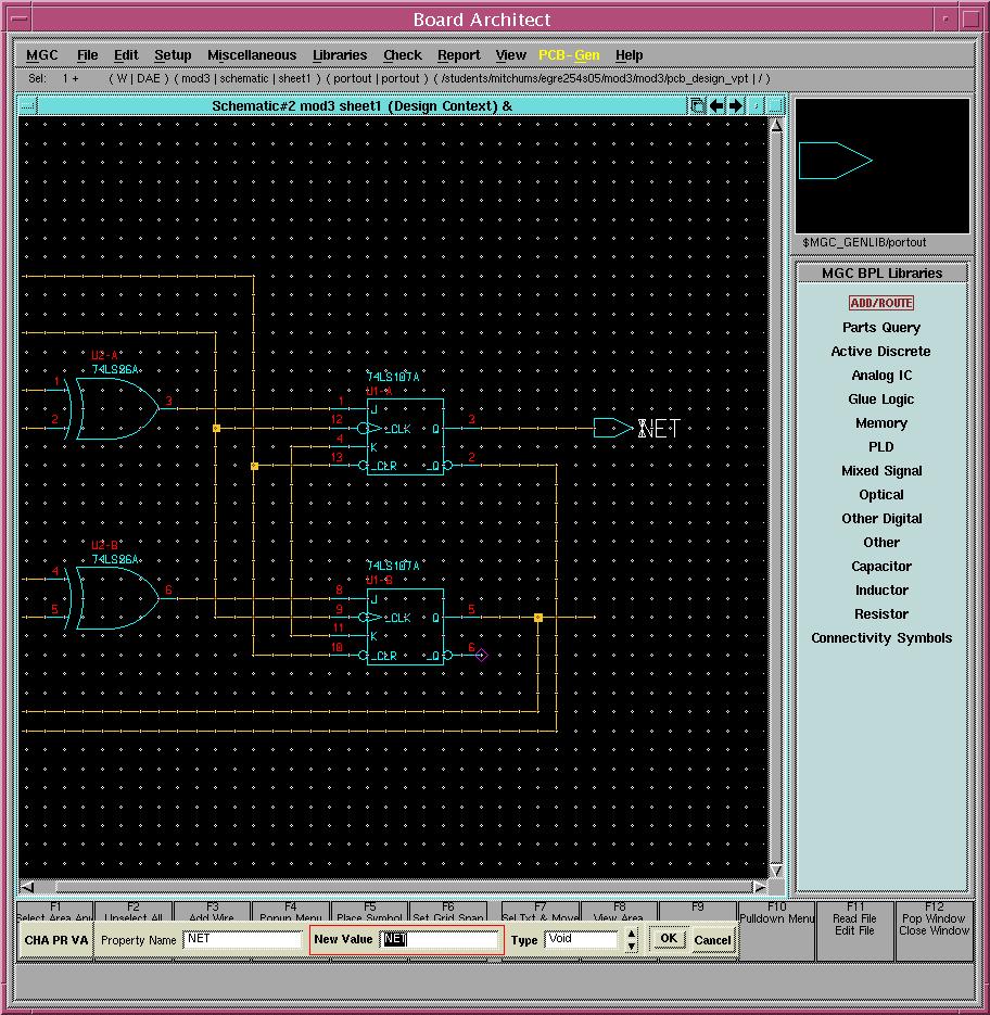
17) You do not need to click or move the mouse. Just type in the new name for this net, Q1, then press the Return key. The name of this output port will change to Q1. Hint: you could also use the Properties->Net Properties->Net Properties command to change the net name but this method is much easier. As when placing parts, left-click once on the portout figure in the top right corner to place another output port. Attach this port to the output of the lower flipflop and change the net name to Q0. F2 to deselect and your schematic should look like:

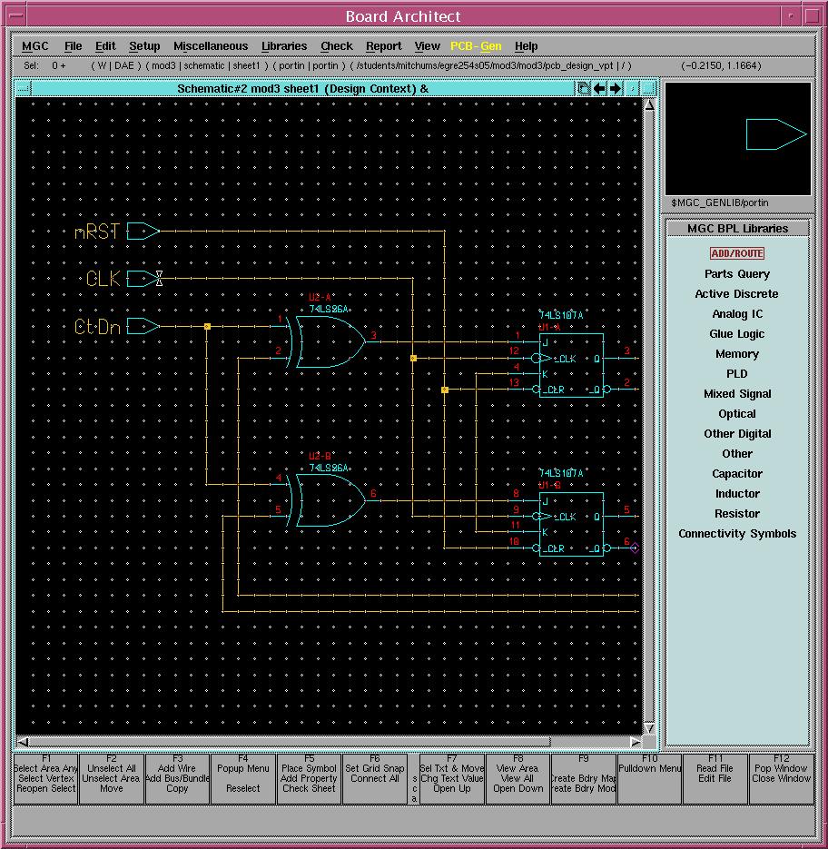
18) Now go back to the Connectivity Symbols dialogue box, pick portin (input ports), add them to the input wires and rename them as shown below. Remember you can use the scrolling bars to move around the schematic. Note you have created an input pin and assigned an input port for the RESET signal: nRST. You do not have to create an input port on the reset signal in order to force a value in the simulator but having one will help you remember to define the force.
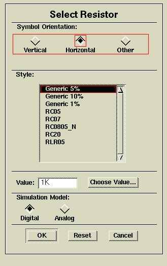
19) Now you will add a couple of pullup resistors. Sometimes it is necessary to use only one input of a gate or flipflop and keep the other input at a high voltage. It is bad practice to leave inputs unconnected, though it is sometimes done with LS logic. It is also undesirable to connect a LS input directly to +5 Volts. So a resistor is used to limit current pulled by the input. The value is not too important, 1K to 10K are standard pullups for LS logic. To add a resistor, select Resistor from the schematic palette on the right. You will see the Select Resistor dialogue box. Fill it in as shown then click OK.
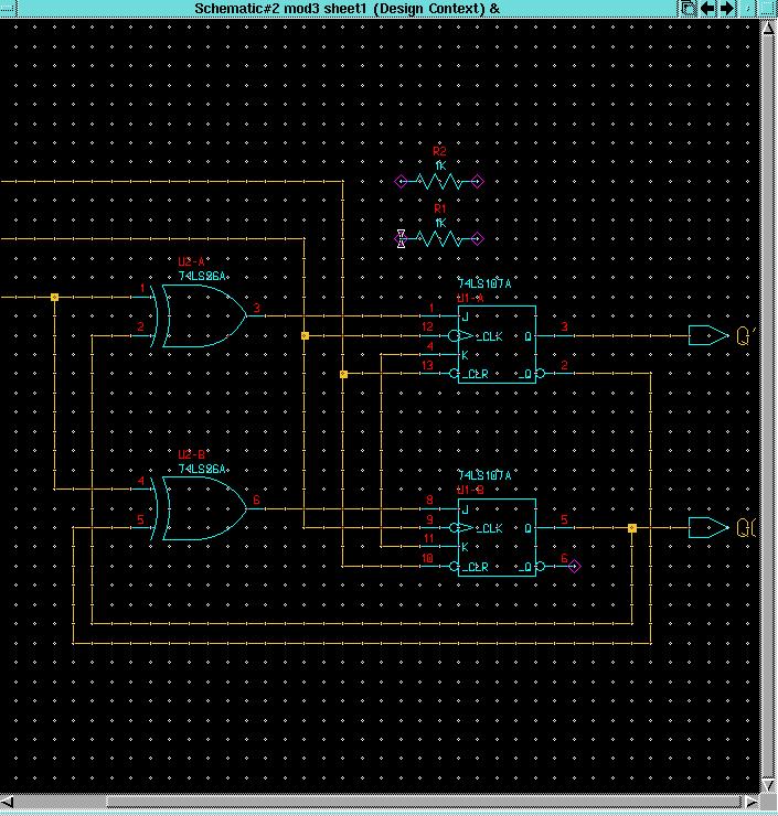
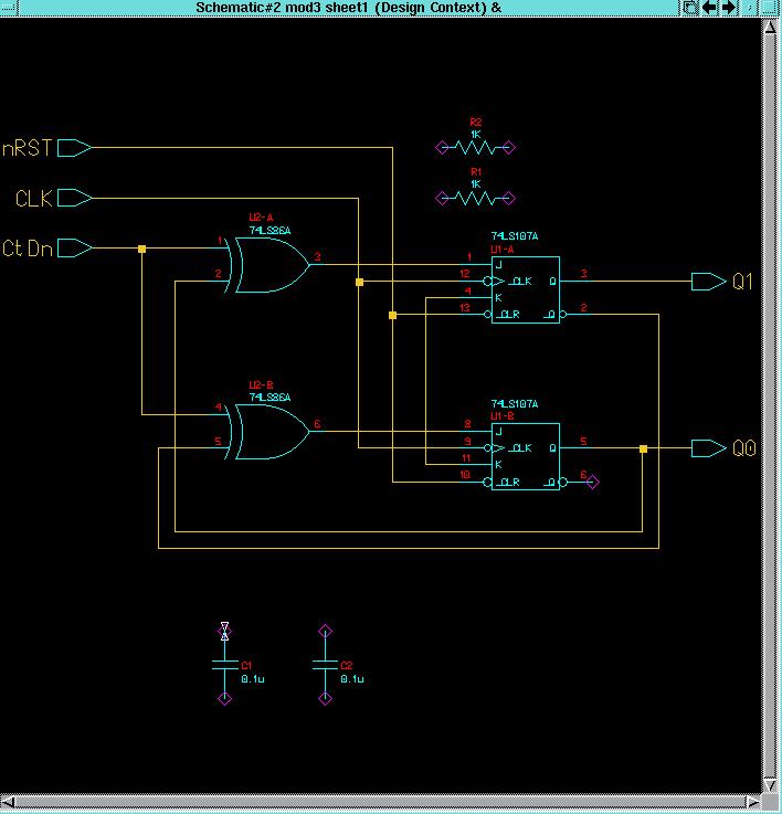
20) Place two resistors as shown below:
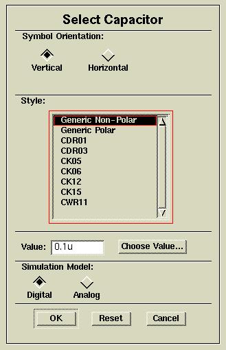
21) It is also good practice to add capacitors across the power supply terminals of each IC. When a digital circuit switches, it creates a high current for a short amount of time. These switching currents generate a lot of noise in the power supply. Placing a capacitor across the power supply leads for each IC will filter a lot of this noise. You have two ICs (one dual flipflop -U1- and one quad XOR -U2-) so you will need two capacitors. The location on the schematic is unimportant. Filter caps (sometimes called decoupling caps because they decouple the AC noise from the DC supply) are typically shown at the bottom of the schematic page. When the circuit is built, however, they should be as close electrically as possible to the power supply pins for each IC. To place your two filter caps select Capacitor from the schematic palette on the left: You will see the Select Capacitor dialogue box. Fill it out as shown then left-click OK.
22) After placing the caps, deselecting everything (F2)and selecting the View->View All command from the top menu bar, your schematic should look like:
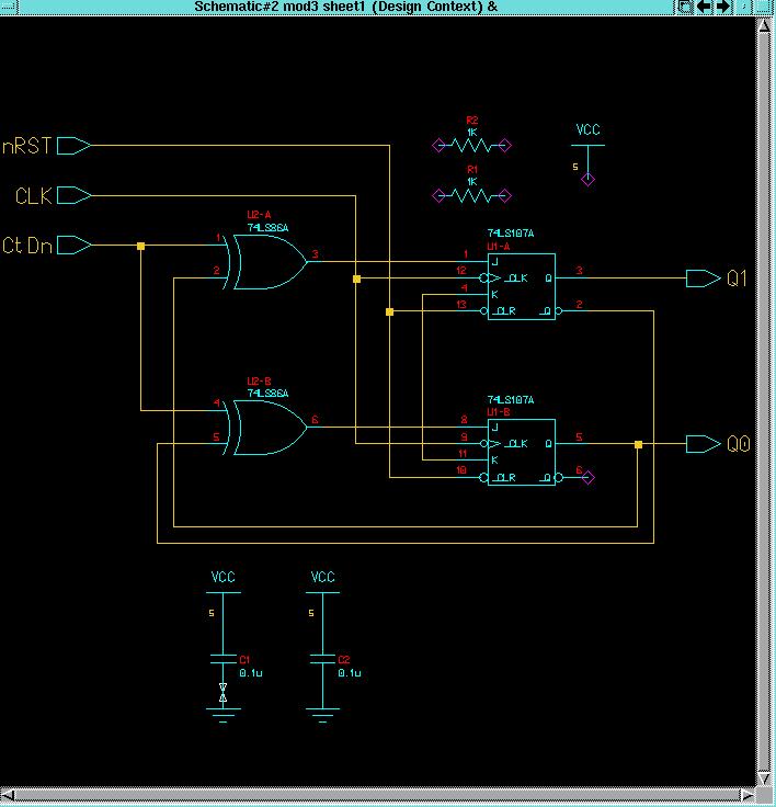
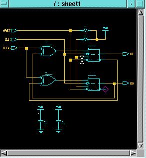
23) Remember the VCC and GROUND symbols are under the Connectivity Symbols menu item on the right hand side of the schematic. (VCC is a common term for the +5V supply voltage in TTL logic). You need to place GROUND connections at the bottom of the caps, VCC connections at the top of the caps and a VCC connection for the two pullup resistors. Add them as shown below:
24) Now you just need to finish wiring up the pullup resistors. From the top menu bar select Libraries->Display Schematic Pallette to return to normal schematic editing. Then choose, as before, the Add Wire icon in the right side menu. Wire the pullup resistors as shown below:
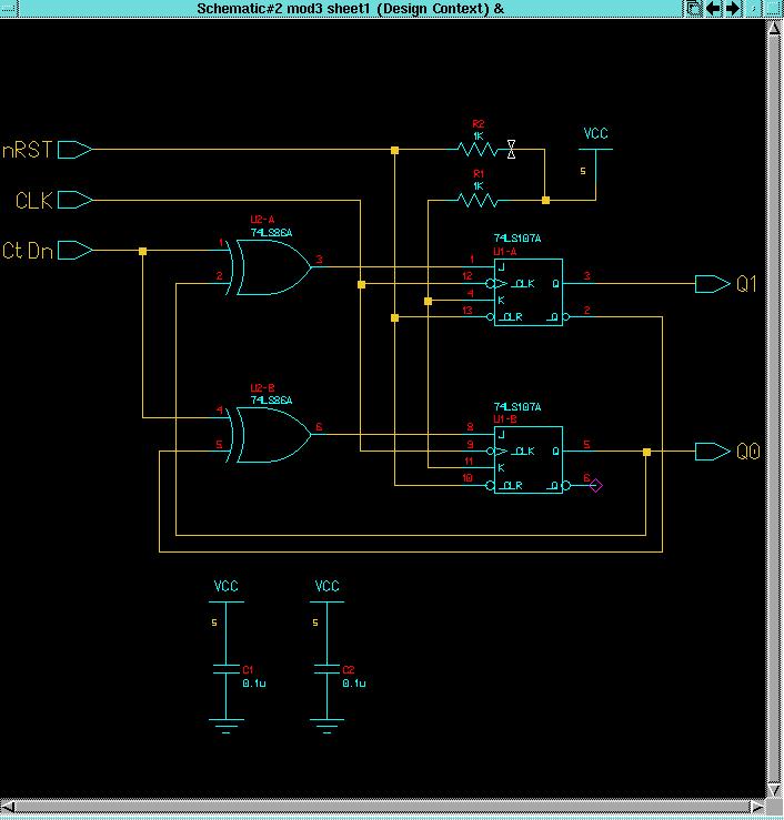
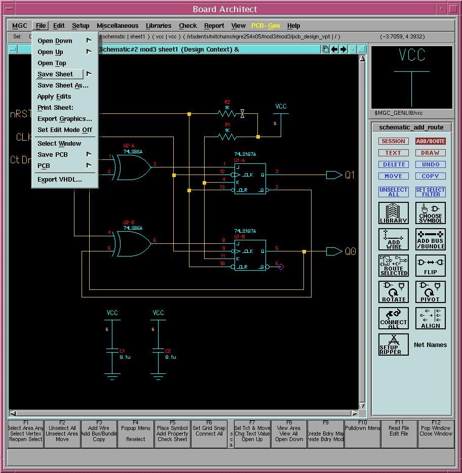
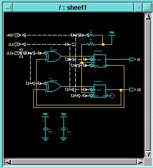
25) Your schematic is finished except for checking and saving. First, save the current schematic sheet. From the top menu select File->Save Sheet like shown below. Do not worry about any options, just left-click once on Save Sheet and Board Architect will save the current schematic sheet you have open.
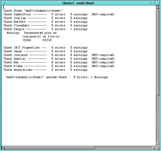
26) Now you should check your shematic to be sure everything is connected like you want it. Board Architect will give warnings or errors if anything is not connected. You have one node not connected (the inverted output of the Q0 flipflop) so you can expect to see one warning. Everything else should be OK. Select from the top bar menu Check->Sheet. You should get a report that looks like the one below. If not, go back and fix any errors. After you fix any errors (or make any changes) remember to go back and save the sheet (File->Save Sheet) then check the design again (Check->Sheet). Hint: If you have added then deleted several components you may get annotation errors. If so, from the top menu bar select Miscellaneous->Clear Unattached Annotations and Board Architect will remove any remnants of the deleted parts from the database. Then Check->Sheet again.
27) Close the check report window by either left-clicking twice on the top left button of the report window or left-click once and select Close.
28) Now we will use Board Architect to create
a net list. A net represents a node (one or wires connected together)
in the schematic. For example, the connection between U1-A pin 1
and U2-A pin 3 is a net. Board Architect keeps up with all the nets
in the circuit. Having Board Architect write out the list of nets
for you is a convenient way to make sure you know how to wire this circuit.
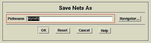
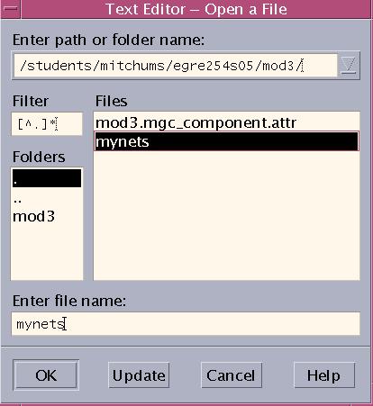
Select File->Save PCB->nets As to generate a netlist. You
will see another popup menu asking for the name of the file where the netlist
will be written. Type in mynets for the filename as shown then left-click
OK.
29) Now you can use a text editor to view the net list file and print it. Move to the bottom control panel on the Unix screen and left-click once on the small arrow above the notecard:

30) You should see a popup menu as shown:
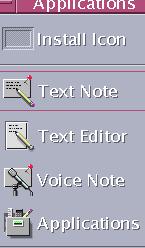
31) Left-click once on the Text Editor item to open a text editor. Be sure you select Text Editor and not Text Note!!!
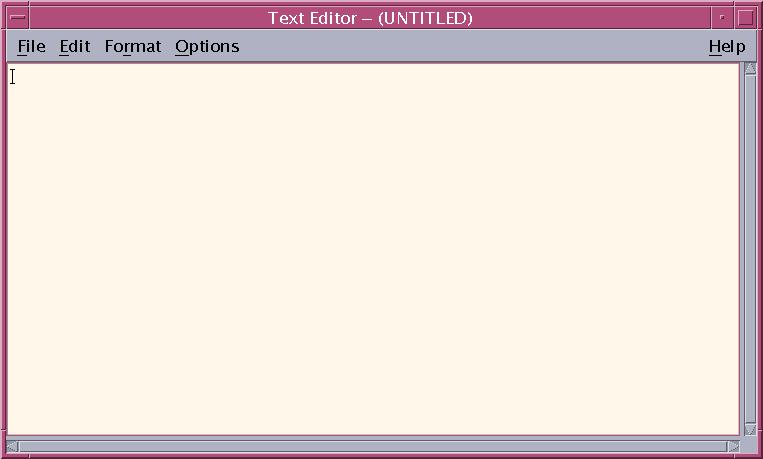
32) Inside the text editor choose File->Open. You will see the open dialogue box. Navigate to the directory containing your design, mod3. Then select the file mynets. Your dialogue box should look similar to this:
33) Click OK to open the net list. Your text editor display should look something like this though the order of the connections may be different:
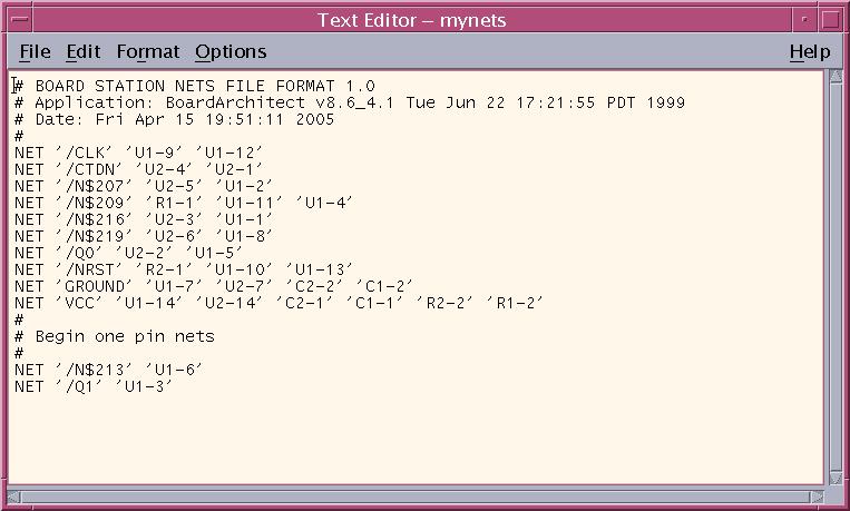
34) Notice each set of connections is called out in a NET statement. The format is: NET 'netname' 'chip-pin' 'chip-pin' etc. You can use this net list to wire the circuit. From the net list you can see that you need to connect a wire from U1-9 to U1-12, for example. Notice also Board Architect is telling you to connect VCC (+5 Volts) to pin 14 of each IC (U1-14, U2-14) and to the tops of the capacitors and resistor (C2-1, C1-1, R2-1 and R1-1). Using a wire list to check your prototyping is a lot easier than trying to read and wire a complicated schematic and can save you a lot of time in lab.
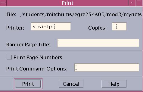
35) You can print the netlist and take it into the 254 lab to help you wire the circuit. It is easier to wire from the netlist than from the schematic for large circuits.. Choose File->Print from the text editor menu bar. You will see a print dialogue box like below. You do not need to change anything; just left-click on the PRINT button.
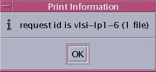
36) The text editor will show the print information dialogue box to inform you about the pending print. Left-click once on the OK button to acknowledge the message.
37) Close the text editor by selecting File->Close.
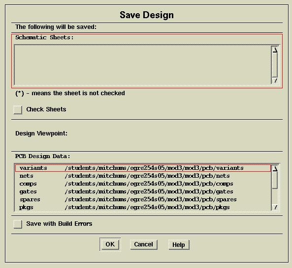
39) This will bring up a Save Design window as shown below. The defaults are fine. Left-click once on the OK button to save your entire design.
40) After the design has been saved, close Build Architect by selecting MGC->Exit from the top menu. (If you need to change the design, start BA again then select File->Open->Set Viewpoint or left-click on the Set Viewpoint icon. This time left-click on the Existing Viewpoint button and navigate to the mod3 component, pcb_design_vpt. Whenever you want to work on the schematic, you must use Set Viewpoint to open the design. This is different from Design Architect - and is what allows Board Architect to keep track of ICs and pin numbers for you.)
42) Now you can start Quicksim as you did in tutorial 1 by typing the following command line: quicksim -tim typ tut & then press the Return key.
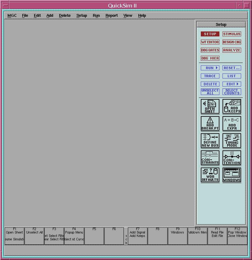
![]()
43) You should see the opening screen for Quicksim as shown:
44) Use the Open Sheet icon or File->Open Sheet to open your schematic. You will get a small window containing your schematic as shown:
45) As before, you need to tell Quicksim what signals to trace in the timing diagram. Make sure the schematic window is highlighted (the border is torquise - not gray) then use the mouse to select signals nRST, CLK, and CtDn. You may left click once on each signal to select it or you may draw a box around one or more signals to select them. Selected signals appear dashed as shown below:
46) Once you have selected all three input signals,
add them to the trace list by either clicking once on the TRACE
palette item ![]() or by right clicking once inside the schematic window then selecting Add->Traces
from the popup menu. Now highlight the schematic window again by
left clicking once on the top bar then press F2 to deselect the
input signals. Select the two output signals and add them to the
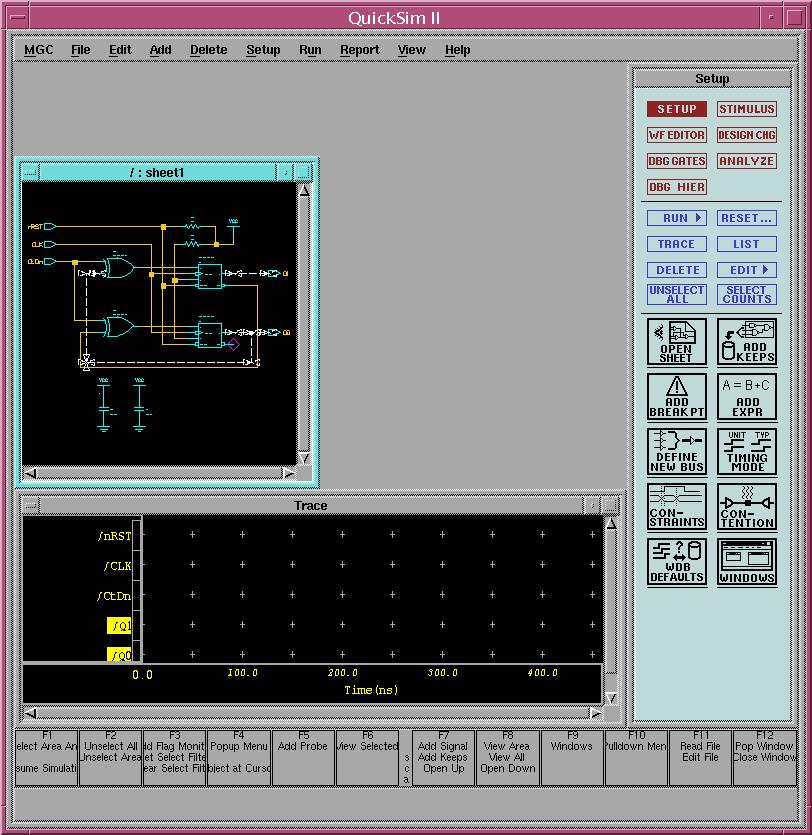
trace as you did the input signals. Now your Quicksim window should
look like:
or by right clicking once inside the schematic window then selecting Add->Traces
from the popup menu. Now highlight the schematic window again by
left clicking once on the top bar then press F2 to deselect the
input signals. Select the two output signals and add them to the
trace as you did the input signals. Now your Quicksim window should
look like:
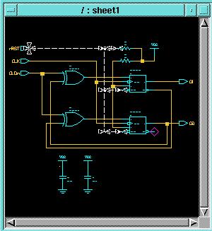
47) Now you must assign forces to the inputs. First make sure the schematic window is highlighted. Then press the F2 key on the keyboard to deselect everything. Now you will add a force to signal nRST. (A force is how you describe an input signal to the simulator.) The nRST signal is a little tricky as we have tied a pullup resistor to it. Select signal nRST by either left clicking on the signal or holding the left mouse button down and drawing a box containing only signal nRST. Your schematic box should look like:
48) As in tutorial 1, you will add a multiple value force. Right click once inside the schematic window. Then right click once on the small arrow to the right of the popup menu item Forces and select Multiple Values. (Alternatiive: From the top menu bar select Add->Forces->Multiple Values.) A multiple value force is simply one where the input is not constant. You should see the following:
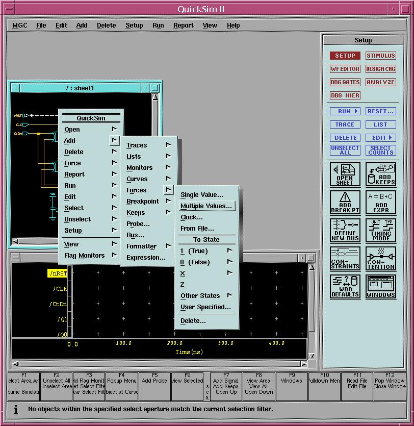
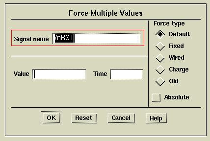
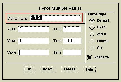
49) Now you should see the Force Multiple Values dialogue box:
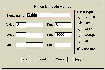
50) Fill in the dialogue box with the values 0, 0, 1, 3000. You can use the TAB key to move to the next location. As you enter force values, the dialogue box expands automatically. This tells Quicksim to apply a logic 0 (0 volts) to the nRST signal at time 0 then apply a logic 1 (5 Volts) at time 3000 nanosecs. Select the Absolute checkbox to indicate you are entering absolute times. Note you must also select the Fixed checkbox because the nRST signal is attached to a pullup resistor. Your completed force dialogue box should like the one below. When you have finished then left-click the OK button.
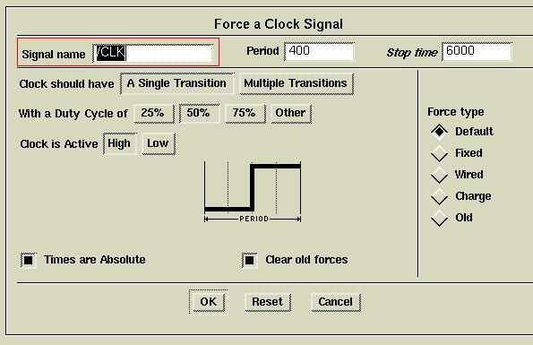
51) You still need to provide an input signal for CLK and CtDn. So press F2 on the keyboard to deselect nRST. You will setup signal CLK as a clock. Select signal CLK. Now right click once in the window, then once on the arrow beside Forces as before. But this time select Clock from the Force popup menu. You will see the Force a Clock Signal dialogue box as shown below. Fill in the dialogue with Period = 400 and Stop time = 6000 and check the Times are Absolute checkbox. These values tell Quicksim to toggle the CLK signal every 200 nanoseconds (for a 400 ns period) and to stop the clock after 6000 nanoseconds. Make your dialogue box look like the one shown then click OK.
52) Now you have only to define one other input signal, CtDn. You want it to be low for half the time then high for the other half. You can either define it as a clock with period 6000 and Stop time 6000 or you can define it as a Multiple Value force. This example uses a Multiple Value force. Since there is no pullup resistor, you can accept the default Force type as shown:
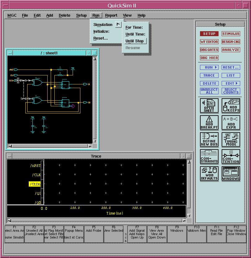
53) Now you are ready to run the simulation.
You can either select (from the top Quicksim menu bar) Run->Simulation->Until
Stop or you can press the RUN button ![]() on the right hand simulation menu then choose Until Stop.
Below is what the top menu bar selection would look like:
on the right hand simulation menu then choose Until Stop.
Below is what the top menu bar selection would look like:
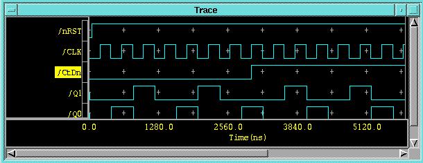
54) You should get a simulation trace similar to the one shown here:
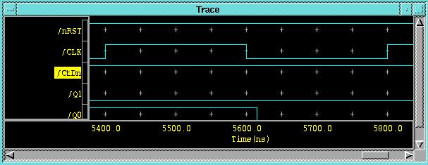
55) Make sure you have selected the Trace window (left-click once beside the title Trace) then you can use the View->All command to expand the trace to the entire window. Note the Modulo 3 counter starts at 00 (it is reset) then counts on the falling clock edges 01, 10, 00, 01, 10, 00 until the CtDn signal goes high. At that time it counts backwards: 00, 10, 01, 00, 10, 01... Your completed, expanded trace should look like:
56) You can print the trace, as in Tutorial 1, by first highlighting the Trace window then selecting File->Print->Active Window. You will see the Print Traces dialogue box. Enter mgcprint for the printer name as shown:
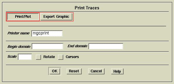
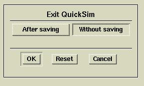
57) Then select OK to print the trace. Being able to simulate a prototype before you build it is very powerful as it eliminates a lot of debug time. If you verify your design is correct before you try to build it then all errors in the lab are either wiring errors or bad ICs. If you don't simulate before building, you will not know if your circuit is designed correctly. Close the simulator by selecting MGC->Exit from the top menu. Select Without Saving in the Exit Quicksim dialogue box as shown:
58) Select OK to terminate Quicksim.