Design for Actel FPGAs Using Schematic Capture
1. What you will learn
1.1. How to create a schematic and symbol for an Actel part.
1.2. How to functionally simulate the Actel part by itself.
1.3. How to place and route the Actel part.
1.4. How to perform a timing simulation on the Actel part by itself.
1.5. How to create a board level schematic that contains both Actel
parts and MGC library parts.
1.6. How to create a design viewpoint for the board level design that
contains back annotated timings for the Actel part.
1.7. How to simulate the board level schematic.
2. Setting up your environment
2.1. First, it is recommended that you create an separate directory
under your class account to hold the designs for EGRE426:
>>mkdir egre427
2.2. The documents referenced in this tutorial are available on-line
in Adobe PDF format. The documents can be viewed by using the command:
>>acroread /mentor/actel/doc/manuals.pdf
Please do not print out the documentation. If a hard
copy of the documentation is needed, see the instructor.
2.2. Note that information on the details of using the Mentor Graphics
Design
Architect (DA) , Quicksim , QuickHDL , and
Renoir
tools is not contained in this tutorial. See the available Mentor Graphics
on-line documentation for tutorials and user's guides for these tools.
3. Create the schematic and symbol for an Actel
part
3.1. Create a tutorial directory under your egre427 directory and start
Design
Architect ( DA ) in it:
>>cd egre427
>>mkdir tutorial
>>cd tutorial
>>act_da &
3.2. Open up a new sheet for this design by pressing the Open Sheet
button in the palette on the right and call it "full_adder." Open up the
parts library for the Actel parts by selecting the Libraries->Actel
Libraries item from the pull down menus and clicking on ACT1
in the schematic palette. This will bring up an alphabetical list of available
macros. The details of these macros can be found in the Actel Macro Library
Guide (/mentor/actel/doc/libguide.pdf).
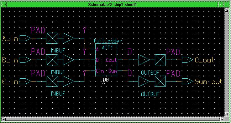
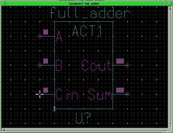
3.3. Use DA to construct a schematic of a single bit full
adder from Actel parts that looks like the one shown in the figure below:
Notice that each input and output has portin and portout parts from
the MGC gen_lib library.
3.4. Check the sheet using the Check->Sheet pull down
menu item. Ignore the warnings that come up in the Check window:
Warning:
Unable to evaluate property "model" on I$3
Unable to evaluate expression
Unable to resolve expression symbol als_technology
Warning: Unable to evaluate
property "__qp_prim" on I$3
Bad Triplet CASE Control Expression
Unable to evaluate expression
Unable to resolve expression symbol als_technology
...
Save the sheet using File->Save Sheet
the pull down menu item.
3.5. Create a symbol for your design using the menu
command Miscellaneous->Generate Symbol... Click OK
in the dialog box that comes up (leaving the default settings), and new
symbol window will come up with the symbol of your part in it.
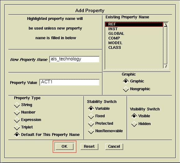
3.6. Add the property als_technology with
the value ACT1 to the symbol by selecting the symbol body (the box)
and selecting Properties->Add->Add Single Property... from
the pop up menus (right mouse button).
Fill in the Add Property dialog box as shown below and click
OK
:
Place the property inside the symbol body after you close the dialog
box.
It is a good idea, although its not required, to add
inst and
comp
properties to the symbol at this time. The
inst property allows
you to give each instance if this part that you place in a schematic a
unique name. This makes it much easier to trace problems later in the design
flow as all the tools will use this name when referring to the location
of a problem (instead of the cryptic I$XXX default inst properties
DA
assigns if you don't add one). The comp property allows you to put
the name of the part on the symbol which makes schematics which use it
more readable.
3.7. With the symbol body still selected, use the Properties->Add->Add
Single Property... item from the pop up menu to bring up the Add
Property dialog box again. Select
INST from the Existing
Property Name selection box and type in U? in the Property
Value box. Click OK and place the property under the
symbol body. Repeat the process selecting the COMP property and
adding the full_adder value and place the property above the symbol
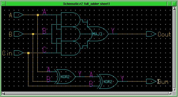
body. The resulting symbol should look like the one shown below.
3.8. Check and Save the symbol and close the symbol window.
Bring up the schematic window and check your sheet again, this time using
Check->Schematic.
In addition to the normal checking of the sheet, the Check->Schematic
command checks to ensure that the ports on the symbol match the ports present
on the schematic sheet. Because the symbol was created automatically by
the tool, one would not expect any errors, but it is a good idea to always
use Check->Schematic when there is a corresponding symbol
for a schematic sheet. Notice that no errors or warnings appear in the
Check
window this time because the als_technology property was added to the symbol.
Save the sheet and exit DA .
4. Create a schematic for a complete FPGA
Before an FPGA design can be placed and routed using
the Actel tools, input and output I/O pad buffers from the Actel library
must be added to the design.
4.1. Open up a new sheet for this design by selecting Open Sheet
and
call it "chip1." Use the Choose Symbol button to select the
full_adder
symbol and place it on the sheet. Add Actel
inbuf and outbuf
parts from the ACT1 library and portin and portout parts
from the gen_lib library to the design's inputs and outputs as shown below.
4.2. Create a symbol for the chip1 part and add the als_technology
property and the optional inst and comp properties as before.
Check and Save the symbol and sheet as before.
5. Functionally simulate the full FPGA design
All designs should be simulated before placement and
routing to ensure that the design is functionally correct.
5.1. Run the presimvpt tool on the chip1 design
to prepare a viewpoint for functional simulation:
>>presimvpt fam:act1 chip1
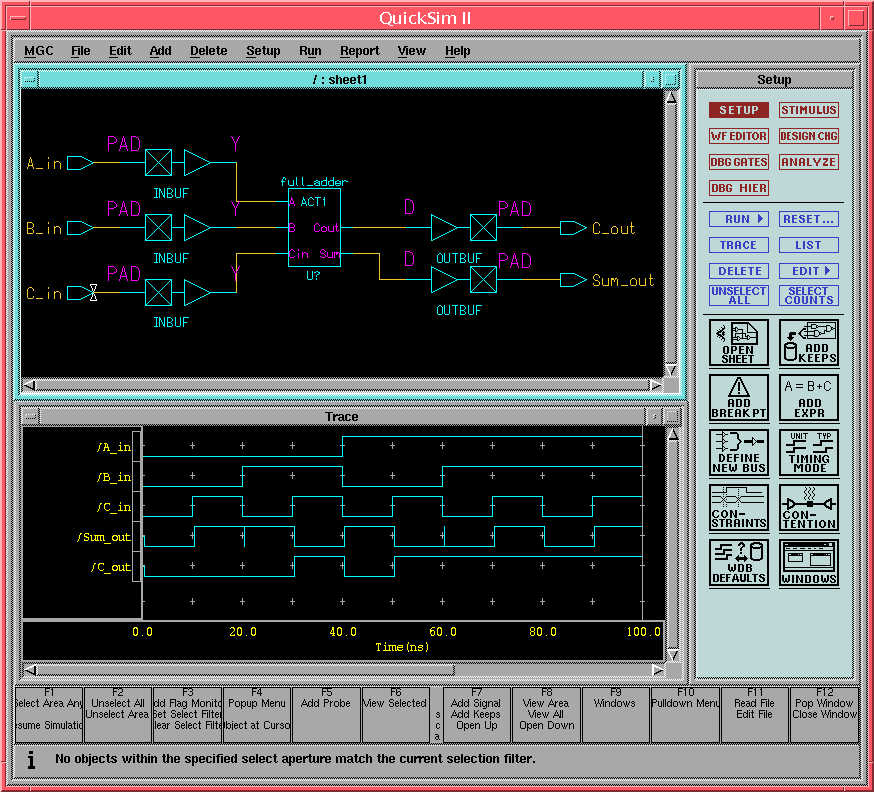
5.2. Invoke the Quicksim simulator on the design:
>>quicksim chip1 &
When the simulator window appears, use the Open
Sheet button to bring up the schematic of the design. Select all
of the nets on the top level of the sheet and use the Add->Traces
item
from the pop up menus to trace the signals in the design. Use the Force->Multiple
Values... menu item to force a sequence of values on the A_in
, B_in , and C_in signals to test the full adder and then
run the simulator for the proper amount of time. Note that because there
are no timing values for the design because it has not been placed and
routed yet, the outputs will not have propagation delays. Therefore, only
a small amount of simulation time is needed between different input values.
The resulting Quicksim window should appear like the one below.
Note that you can create a command file for Quicksim
(called a "dofile") with commands that will open the sheet, trace specified
signals, force values on specified signals, and run the simulation. Creating
a dofile is very useful when debugging complex designs that may take many
simulation runs to verify. You can perform the functions manually the first
time and then capture the proper syntax for them in the transcript window
(the window in which Quicksim was invoked), or check the
Quicksim
manuals in the Bold Browser for the syntax of commands in a dofile.
6. Place and route the Actel part
Placement and routing begins with the creation of an
EDIF
netlist from the DA schematic. This EDIF netlist is
then imported into the Actel Designer tool for placement
and routing.
6.1. Create the EDIF netlist for the Actel place and route tool from
the Mentor schematic:
>>mgc2edn fam:act1 chip1
Note that this process calls a number of separate tools
including Mentor's Design Viewpoint Editor (DVE) . No errors or
warnings should result from this process.
6.2. Start the Actel Designer tool:
>>designer &
6.3. Chose File->Import->Netlist File...
from the menus and click on New in the Import or Open
dialog
box that pops up.
In the Import Netlist dialog box, click on the
Browse...
button and select the chip1.edn file under the chip1 directory.
Click the OK button in the Import Netlist
dialog box and make sure that the ACT1 family is selected
in the Setup Design dialog box that comes up and then click OK
in it.
In the Designer main window, click on
the Compile button.
6.4. Select A1020B , and 84PLCC from the
Device
Selection dialog box that pops up and click OK in the Operating
Conditions dialog box when it appears. The compile procedure
may generate warnings or even errors if fanout violations are detected.
Actel primitives have a maximum fanout of 24 devices. The fanout errors
must be corrected by adding buffers to subdivide the affected signals.
No other types of errors should occur. The compile procedure will
also tell you how many of the 547 available logic modules on an Actel 1020B
FPGA your design utilized.
6.5. Select the Layout function in the Designer
main window and select the default options by clicking
OK
in the Layout dialog box that pops up. Note that you can perform
more sophisticated placement and routing functions if necessary to help
fit a design that is near the maximum size into a given FPGA. See the Designer
User's Guide for more details (actel_designer_users_guide.pdf). No
errors or warnings should occur in the layout process.
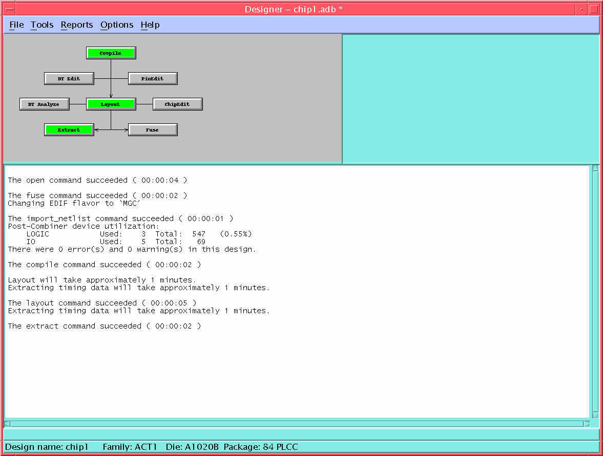
6.6. Select the Extract function in the Designer
main window to extract timing data from the placement and routing results.
Click OK in the Extract dialog box that pops up. You are
now done with the Designer tool. The resulting main window
in Designer should appear like the one below.
Note that if you were going to actually program an FPGA,
you would need to select the Fuse function in the Designer
main window.
6.7. Select File->Save to save the placement and routing
for the design. Add chip1/chip1.adb to the end of the File Name:
entry in the Save As dialog box that appears and click OK
.
7. Perform a timing simulation of the Actel part
by itself
After placement and routing is complete, the Actel design
should be simulated again with full timing information. This will allow
a determination of the clock speed at which the design will run and the
delays that will be seen on the design's outputs.
7.1. Import the timing data and simulation models back into the Mentor
environment:
>>del2mgc chip1
Note that this process also calls a number of separate
tools including DVE .
7.2. Invoke Quicksim on the design:
>>quicksim -tim typ chip1
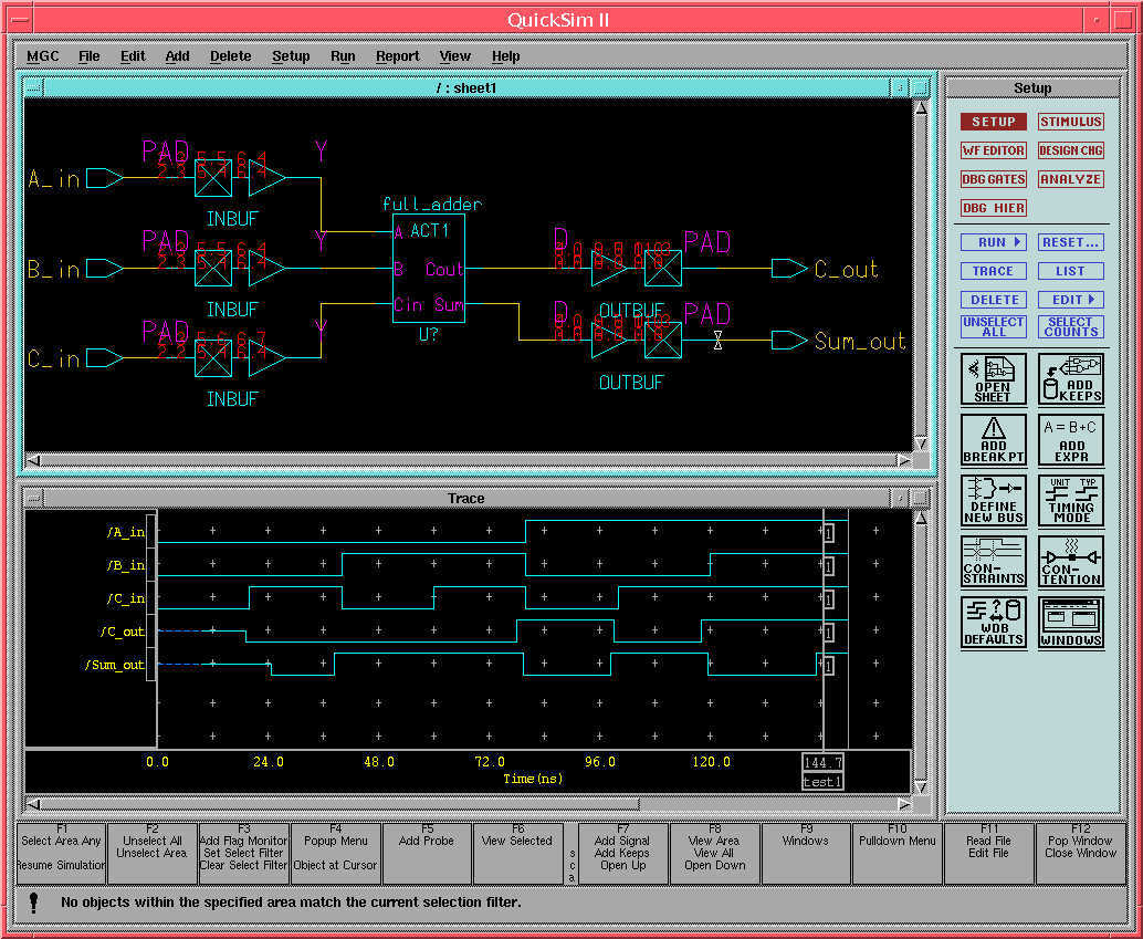
7.3. Trace the signals and add forces as before
to test the design. Note that with timing delays added, it will require
that the design be simulated for a longer period of time before valid values
propagate to the outputs. Cursors can be added to the trace window to measure
propagation times from inputs to outputs. When two cursors are added and
snapped to the edges of signal value changes, the time value shown on the
second cursor is the difference between it and the time of the previous
cursor, i.e., the propagation time of the signal selected. The resulting
Quicksim display should be similar to the one below.
8. Create a schematic for a test board
Once the FPGA design is placed and routed, it can be
used on a schematic of the entire system and simulated there with full
timing delays. In this simple tutorial, a system level schematic consisting
of the full adder FPGA with TTL D flip flops on its inputs and outputs
will be created and simulated for demonstration purposes.
8.1. Restart DA to create the system level schematic:
>>act_da &
Open up a new sheet for this design by selecting Open
Sheet and call it "board1." Place the symbol of the chip1
design on it by using Choose Symbol from the schematic palette.
Open up the parts library for the MGC parts by selecting
Libraries->MGC
Digital Libraries from the pull down menus. Select a quad 74379
D flip flop by clicking on ls_lib and
74ls379
in the schematic palette. Place the symbol on the schematic.
8.2. Complete the schematic so that it looks like the one below.
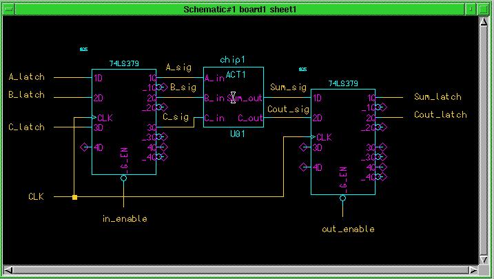
Add two 74ls379 D flip flops, add the nets, and name
them as shown. Change the instance property of the chip1 FPGA from
U?
to U01 by placing the cursor over the property, hitting
<shift><F7>
, and then filling out the pop up dialog box.
8.3. Check and Save the sheet. Close the schematic window
and exit DA .
9. Create a simulation viewpoint for board1 and
backannotate the Actel timings
Every schematic needs to have a "viewpoint" created before
it can be simulated. The viewpoint tells the simulator where to get the
simulation models for the various parts on the board. Normally, when designs
are simulated, Quicksim creates the viewpoint, or for simulating
the Actel parts by themselves, the viewpoint is created by the presimvpt
tool. Because this design has Actel parts mixed with other parts, a specific
viewpoint, that has the post-placement and routing timing values for the
Actel design back annotated to it, must be created with DVE "by
hand."
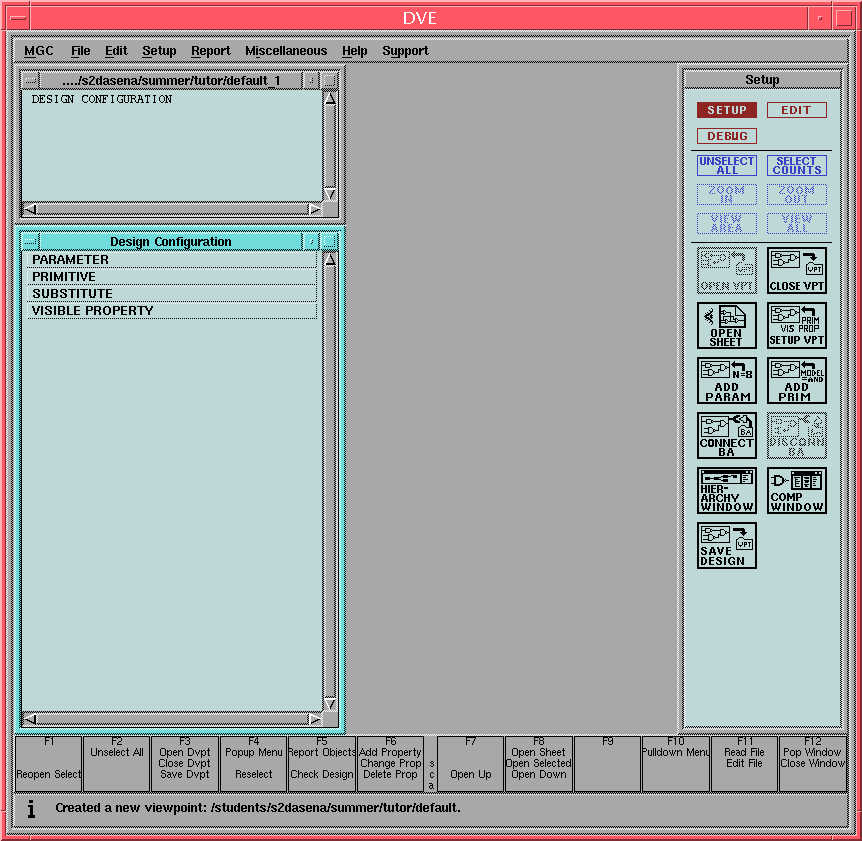
9.1. Start DVE:
>>dve board1 &
9.2. The first time you do this for a specific
design, no viewpoint will exist, so DVE will create one called "default."
The resulting display will be like the one shown below.
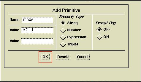
9.3. Select ADD Prim
from the from the palette on the right. Fill in the Add Primitive
dialog box with a new primitive name of model , a value of ACT1
and a type set to string as shown below and click OK:
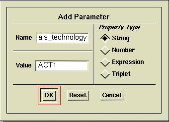
9.4. Select ADD Param from
the from the palette on the right. Fill in the Add Parameter dialog
box with a new parameter name of als_technology , a value of ACT1
, and a type of
string , as shown below and click OK:
9.5. Select ADD Param from
the from the palette on the right again, and this time, fill in the Add
Parameter dialog box with a new parameter name of tsuasync ,
a value of 0 , and a type of string , and click OK
9.6. Select Open Sheet from the palette on the right
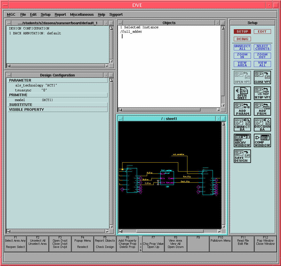
and select the Actel chip1 part on the schematic when it comes up.
From the menus, select Report->Object->Short and position
the window that comes up above the schematic window. This step is needed
to verify the instance name for the Actel part. Because you set the INST
property to "U01" on the schematic, instance name will be /U01. The result
will look like the figure shown below:
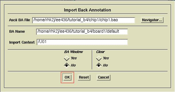
9.7. Select File->Back Annotation->Import...
from the menus. An Import Back Annotation dialog box will come up.
Click on the Navigator... button in the dialog box and then click
on the
 button in the Ascii Back Annotation
Name dialog box. Type in the full path to the chip1 design,
e.g. /home/<your_id>/egre426/tutorial/chip1 and then click OK
in Change Directories To: dialog box. Select the chip1.bao
file when it appears. This will fill in the Ascii BA File portion
of the dialog box. Fill in the Import Context portion of the dialog
box with the instance name of the Actel chip1 part, /U01
. The dialog box should look like the one shown below. Click on OK
. The default back annotation should appear in the design configuration
and no errors or warnings should appear.
button in the Ascii Back Annotation
Name dialog box. Type in the full path to the chip1 design,
e.g. /home/<your_id>/egre426/tutorial/chip1 and then click OK
in Change Directories To: dialog box. Select the chip1.bao
file when it appears. This will fill in the Ascii BA File portion
of the dialog box. Fill in the Import Context portion of the dialog
box with the instance name of the Actel chip1 part, /U01
. The dialog box should look like the one shown below. Click on OK
. The default back annotation should appear in the design configuration
and no errors or warnings should appear.
9.8. Save the design viewpoint by selecting
File->Save
Design Viewpoint from the menus. Exit DVE .
9.9. Start Quicksim on the board1
design:
>>quicksim -tim typ board1 &
Note that no warnings or messages should appear in the
simulation window.
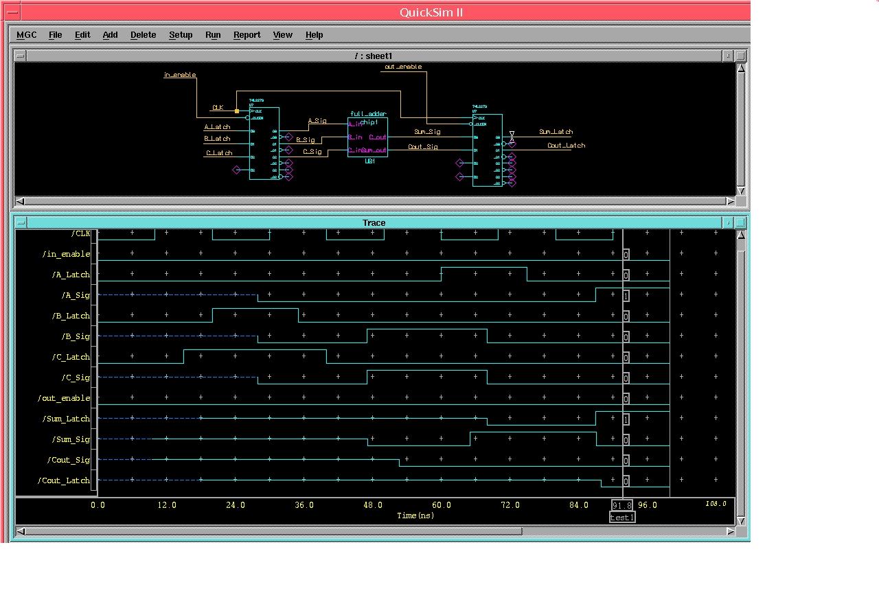
9.10. Open the sheet and add traces for the
signals on the board. Force a clock value on the CLK signal, and
force values onto the inputs to the board. Remember to enable (force a
"0" on the _G_EN input) and disable (force a "1" on the _G_EN
input) the D flip flops at the proper times to latch the inputs and outputs
from the chip1 FPGA. The result should be like the one shown below.
9.11. Exit Quicksim . The tutorial for Lab 1 is complete.