Creating a simple 3.3V Regulator
Circuit using PADS
What you will learn:
- Creating a Circuit Schematic with PADS Logic
- Creating a PCB Design with PADS Layout
- Routing a PCB Design with PADS Router
- Linking PADS Logic to PADS Layout & PADS Router
- Generating Gerber Files with PADS Layout
Note: This tutorial assumes that you've
completed the PADS User Interface tutorial and the New Part Type
tutorial.
1. Creating a Circuit
Schematic using PADS Logic
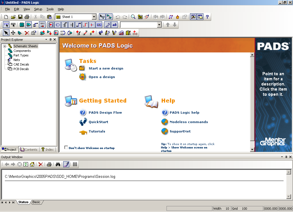
1.1 Begin by opening PADS Logic. Select
Start > Programs
> Mentor Graphics SDD > PADS2005 SP2 > System Design > PADS
Logic.
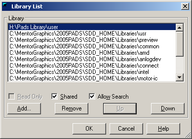
1.2 Ensure that your user library is loaded by using
the library manager -
File > Library.
(Refer to section 3 of the New Part Tutorial for step-by-step
instructions).
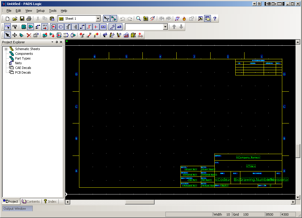
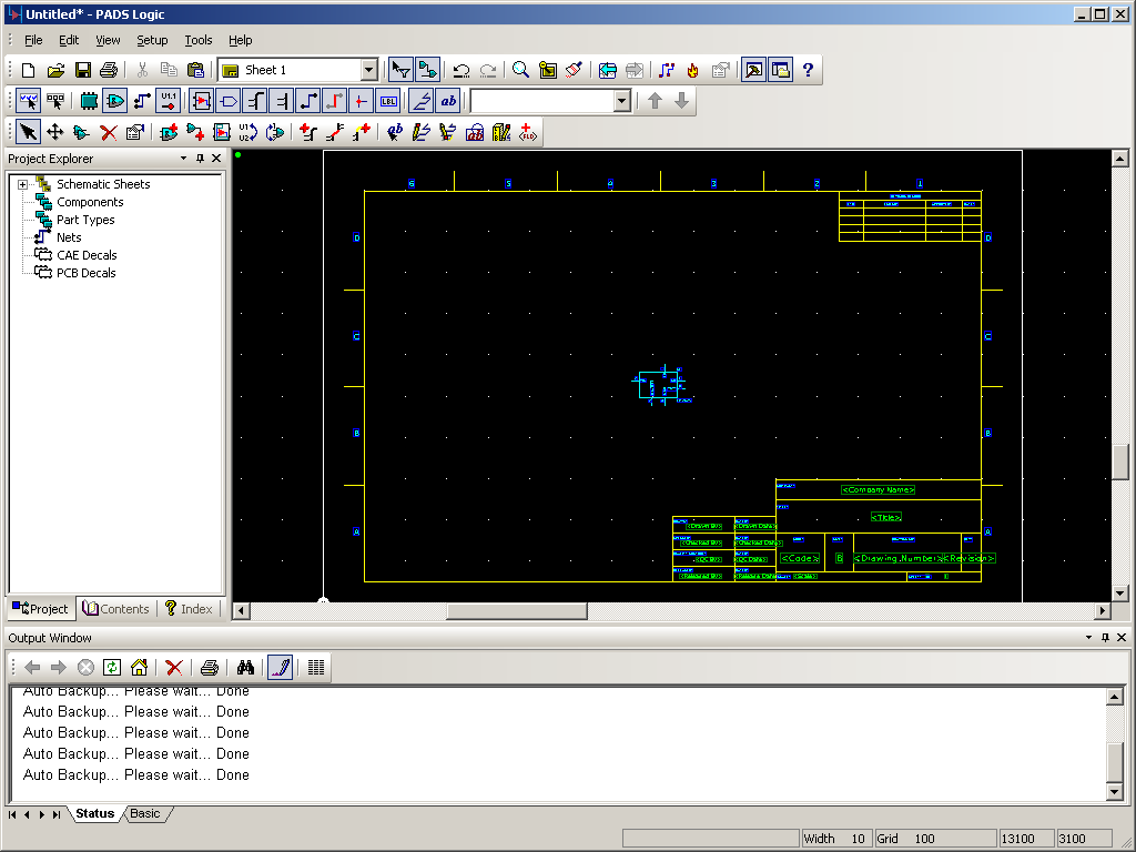
1.3 Start a new design by selecting
File > New.
Your PADS Logic window should look something like this.
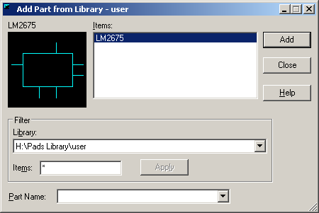
1.4 Use the Add Part window to add an LM2675 voltage
regulator to your design.
To add a part to your design, click on the

button on the
design toolbar. This will open the Add Part from Library window
as shown below.
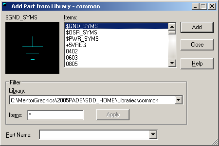
To locate the LM2675 part, you will need to select your custom library
from the Library dropdown list in the filter. Select
H:\Pads Library\user.
Ensure that the Items field contains a single asterisk
* and then
press Apply. This will filter the results, displaying only the
parts in your user library. The window should look like the one
below.
Press the Add button. An outline of the LM2675 part will appear
below the mouse pointer while it is within the design window.
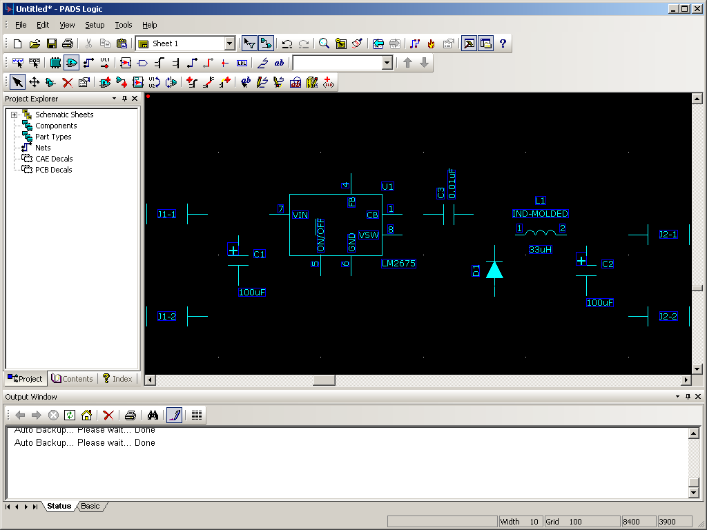
Close the Add Part window and click somewhere near the center of the
sheet to add an instance of the LM2675 part. Press escape to exit
add part mode. You schematic window should look similar to the
one below.
Note: You may wish to zoom in on the LM2675 before completing the
following steps. (Refer to the User Interface Tutorial if
necessary).
1.5 Add capacitors to your design.
Open the add part window by clicking the
button on the
toolbar. In the library dropdown list, choose the
misc library
(C:\MentorGraphics\2005PADS\SDD_HOME\Libraries\misc). In the
Items menu, type
CAP* and
then press Apply. This will filter the results to display only
the parts starting with 'CAP' that exist in the 'misc' library.
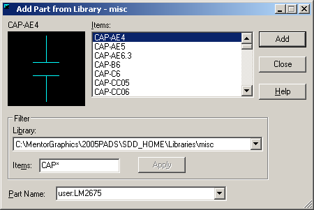
Select the part named CAP7343 from the list and press Add. Move
the Add Part window so that most or all of the design area is
visible. Your screen should look similar to the one below.
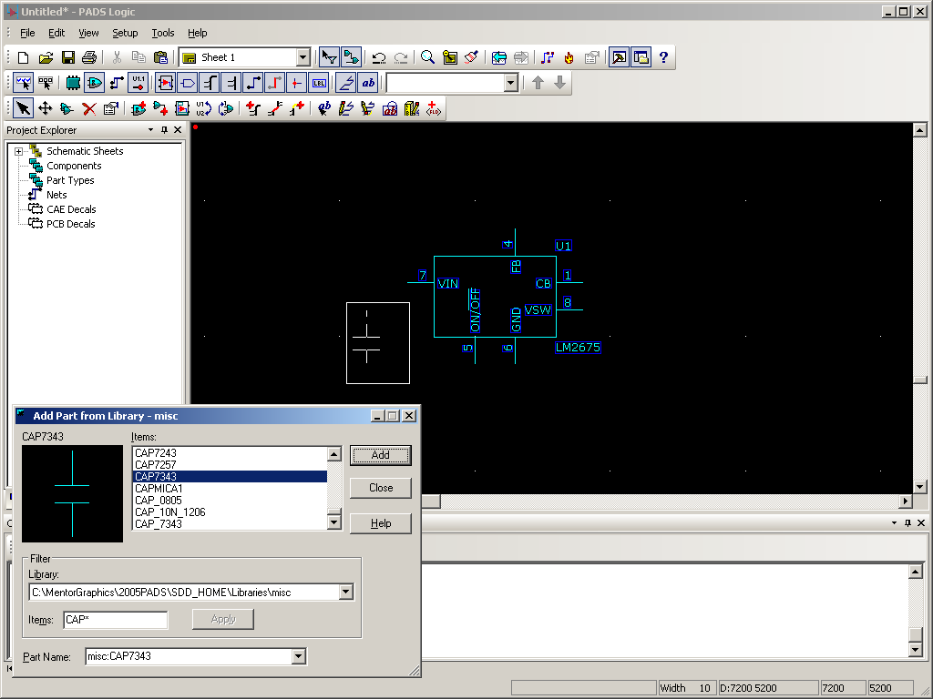
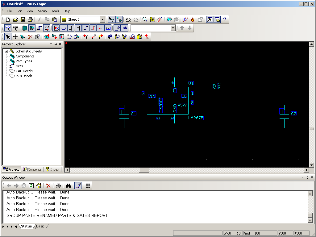
Place the CAP7343 capacitor to the left of the LM2675 as shown
above. Place a second CAP7343 to the far right as shown in the
schematic below.

Now select CAP1206 from the Add Part window, press Add and close the
window. Before adding the capacitor to your design, press
Ctrl + R to
rotate it 90 degrees. Place the capacitor to the right of the
LM2675 as shown below.
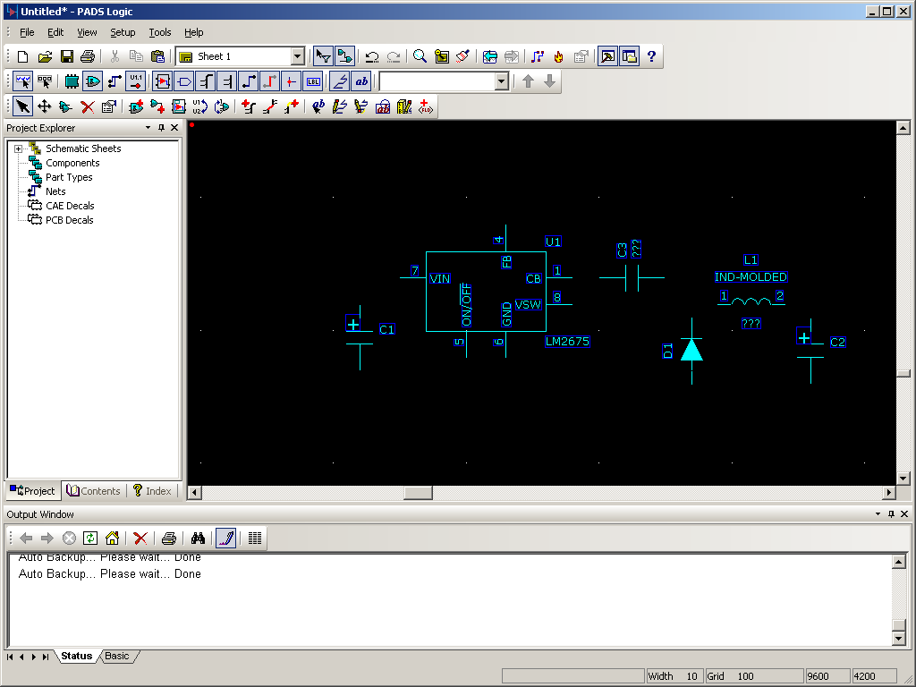
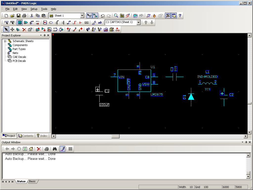
1.6 Add additional circuit components to your design.
Add an inductor and diode to your design as shown in the image
below. Use the IND-MOLDED part for the inductor and the DIODE
part for the diode. Both of these parts are found in the 'misc'
library.
1.7 Assign values to your components.
Ensure that part selection is enabled by right clicking in an empty
area and selecting the
Select Gates
option. This can also be achieved by pressing the

button
on the filter toolbar.
Double click on the left-most capacitor. This will open the Part
Properties window as shown below.
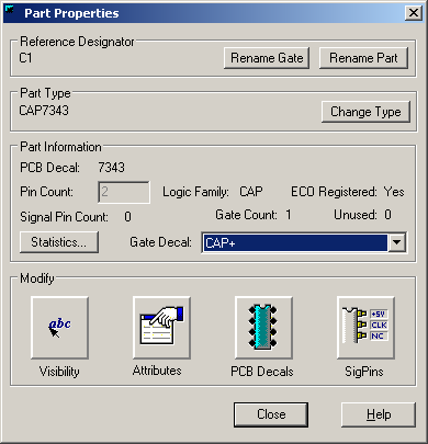
Click on the Attributes button to open the Part Attributes window.
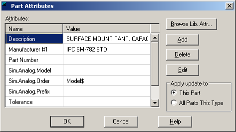
Scroll down to the Value field, double click and enter
100uF in the text box.
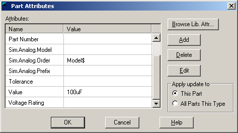
Press OK to close the Part Attributes window and return to the Part
Properties window. By default, the CAP7343 part will not display
its value in the schematic. To change this, click the Visibility
button to open the Part Text Visibility window.
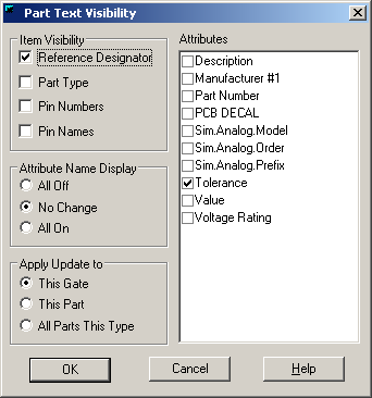
Check the Value checkbox on the right side to enable display of the
capacitor's value. Press OK to close the Part Text Visibility
window and then press Close to close the Part Properties window.
Your schematic should now look like the one below.
Repeat this process for the other components, assigning the values
listed below:
- Right Capacitor - 100uF
- Middle Capacitor - 0.01uF
- Inductor - 33uH

1.8 Change the PCB footprints assigned to the inductor and
diode.
The IND-MOLDED and DIODE parts both default to using through-hole
footprints. We will change these parts to use surface mount
footprints.
Double click the inductor to open the Part Properties window.
Click on the PCB Decals button to open the PCB Decals Assignment window.
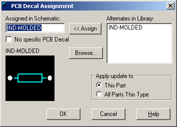
Click Browse... The Get PCB Decal from Library window will
appear. This window functions almost identically to the Add Part
window.
The footprint we will be using for the inductor is named IND7 and is
found in the 'common' library.
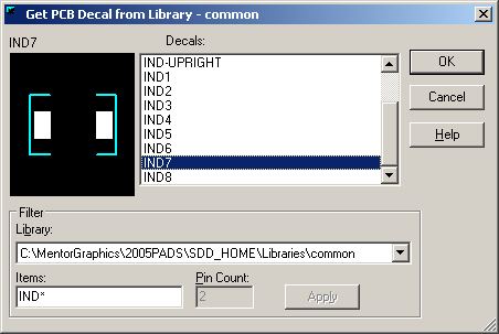
Select this decal and press OK. Then press OK in the PCB Decal
Assignment window and close the Part Properties window.
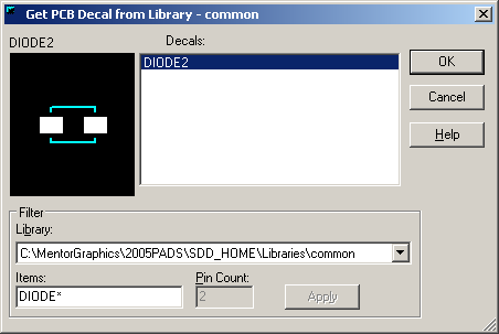
Repeat this process for the diode, selecting the DIODE2 footprint from
the 'common' library.
1.9 Adding Header Pins to your design.
We will now add a pair of 2-pin headers to the schematic. One
2-pin header will be used for the input voltage source (12V), and the
other will be used for the 3.3V output.
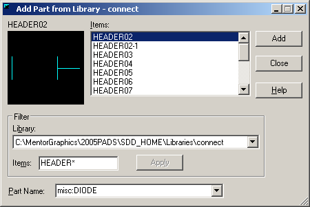
Open the Add Part window. Select the 'connect' library from the
dropdown list and enter HEADER* in the Items filter. Press Apply
and select HEADER02 from the list of parts.
Note: PADS implements connectors as if they were multi-gate IC's.
In this case, each pin is treated as a separate gate and must be added
individually.
Add two header pins to the left of the schematic, and two to the right
(Use
Ctrl+F to
mirror a part horizontally). Your schematic should look similar
to the one below.
1.10 Connecting your parts.
Press the

button on the
design toolbar. This will activate Add Connection Mode.
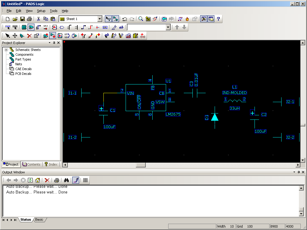
Place the cursor on pin 7 of the LM2675 and click once to begin adding
a connection. Move the cursor to the left until it is
horizontally aligned with the left capacitor. Click once.
This will add a vertex / pivot point to your connection. Move the
cursor down and click on the top terminal of the left capacitor to
complete the connection. Your schematic should look like the
image below.
Continue adding connections until your schematic is fully connected as
shown below.

Note: To remove a misplaced connection, ensure that the selection
filter allows selecting connections. Then click on the connection
you wish to remove and press delete. You can also activate Delete
Mode by pressing the

button on the
design toolbar. This will allow you to remove objects with a
single click.
1.11 Adding Power and Ground Connections
To add a ground connection to your design, enter Connection Mode.
Begin by starting a new connection from the bottom-most net and moving
down 2 or 3 spaces. Then right click and select Ground from the
context menu.
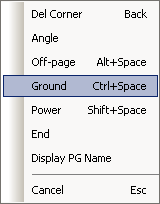
Position the ground symbol at the desired location and click once to
place it.

Adding a power connection is done in a similar manner. Begin by
starting a new connection from the net connected to pin 7 of the LM2675
and moving up. Right click and select Power from the context
menu. Position the power symbol and click once to place it.
Repeat this process for the net connected to the top right header
pin. Your schematic should look like the one below.

By default, all power connections are automatically connected to a net
named +5V. We will need to change this for our design.
Double click on the left power symbol. This will open the Net
Properties window shown below.
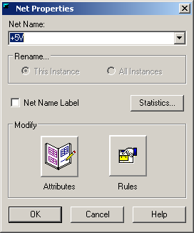
Change the Net Name field to +12V and select the Net Name Label check
box. Press OK.
Repeat this process for the right power symbol, setting the Net Name to
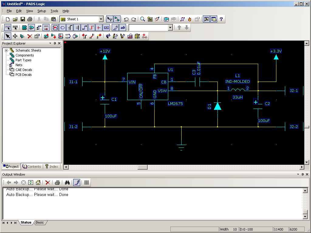
+3.3V. The completed schematic should look similar to the image
shown below.
1.12 Save your schematic. Select
File > Save
and save the schematic to
H:\PADS
Tutorial\Tutorial.sch.
2.1 Linking PADS Logic to
PADS Layout
Before you can begin laying out your PCB, you must transfer the
schematic netlist to PADS Logic. The recommended way of doing
this is to create an application link between PADS Logic and PADS
Layout. In addition to allowing automatic synchronization of the
schematic and layout information, linking also enables a feature known
as cross-probing. This basically allows the selection of a part
or net in PADS Logic to result in the selection of the corresponding
PCB footprint or trace in PADS Layout, and vice versa.
To connect PADS Logic to PADS Layout, select
Tools > PADS
Layout. The Connect to PADS Layout dialog will appear.

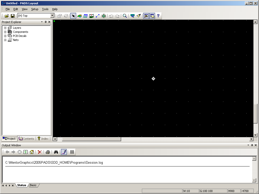
Since we have not yet created a PCB Design file, click the New
button. A new PADS Layout window should appear as shown below.
Note: On subsequent connections to PADS Layout or PADS Router, you will
click Open and select your existing design file.
Note: If you have the available screen real estate, it is recommended
that you resize the PADS Logic and PADS Layout windows so that both are
visible simultaneously. A multi-monitor setup is especially
useful for this.
2.2 Transferring the Netlist from PADS Logic to PADS Layout
Note: Before transferring the netlist, ensure that your custom user
library has be added to Layout's Library List. Refer to the New
Part Tutorial if necessary.
While PADS Layout is still open, switch back to PADS Logic. The
PADS Layout Link window should be visible.

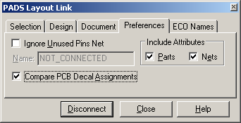
Click on the Preferences Tab and select the Compare PCB Decal
Assignments checkbox. This will ensure that the modified inductor
and diode footprints are properly sent to PADS Layout.
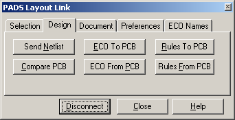
Now click on the Design Tab. Press the Send Netlist button to
transfer your design to PADS Layout.
Switch back to the PADS Layout window. You should now see a
cluster of parts located at the origin (Location 0,0).
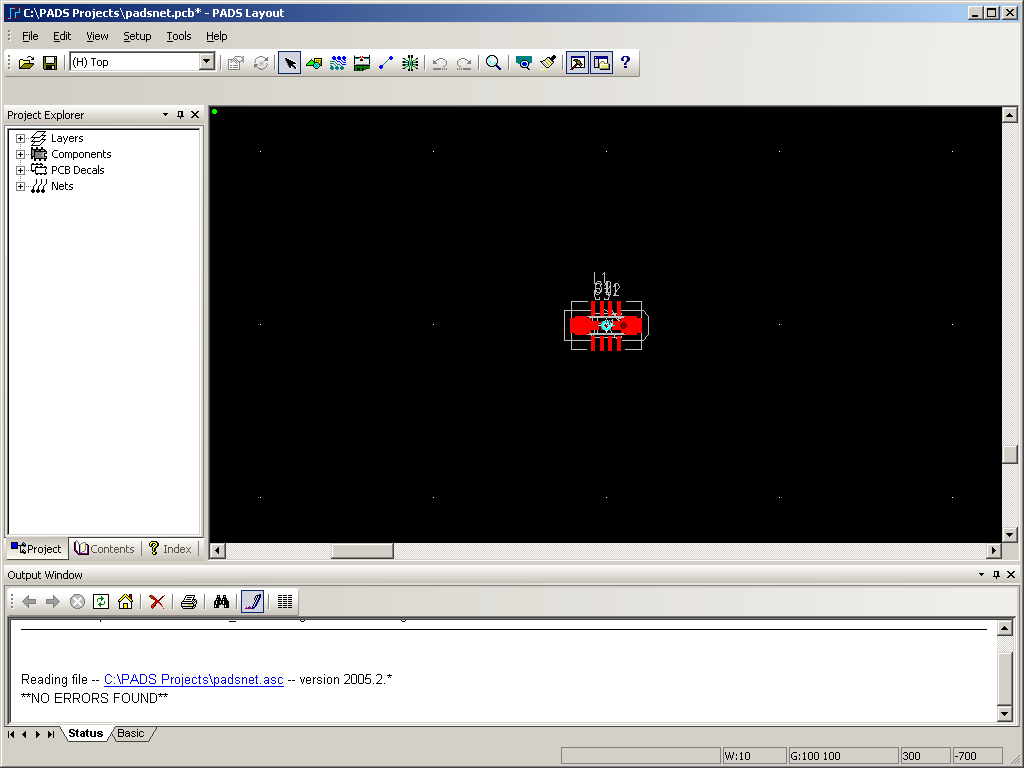
2.3 Creating the board outline.
After transferring the netlist, you will need to create a board
outline. Press the

button to
enable the Drafting Toolbar.

On the Drafting Toolbar, click on the

button to
enter board outline mode.
Since our circuit is extremely simple, a 1.0 inch by 0.7 inch PCB
should be large enough.
Note: For the following steps, refer to the location indicator at the
bottom-right corner of the window. Locations are given assuming
that design units are in mils.
Place the cursor at the origin (location 0, 0) and click once to begin
drawing the outline.
Move the cursor up to location 0, 700 and click once to form the left
edge of the PCB.
Move the cursor right to location 1000, 700 and click once to form the
top edge of the PCB.
Move the cursor down to location 1000, 0 and double click to complete
the PCB outline (forming the right edge and bottom edge of the PCB).
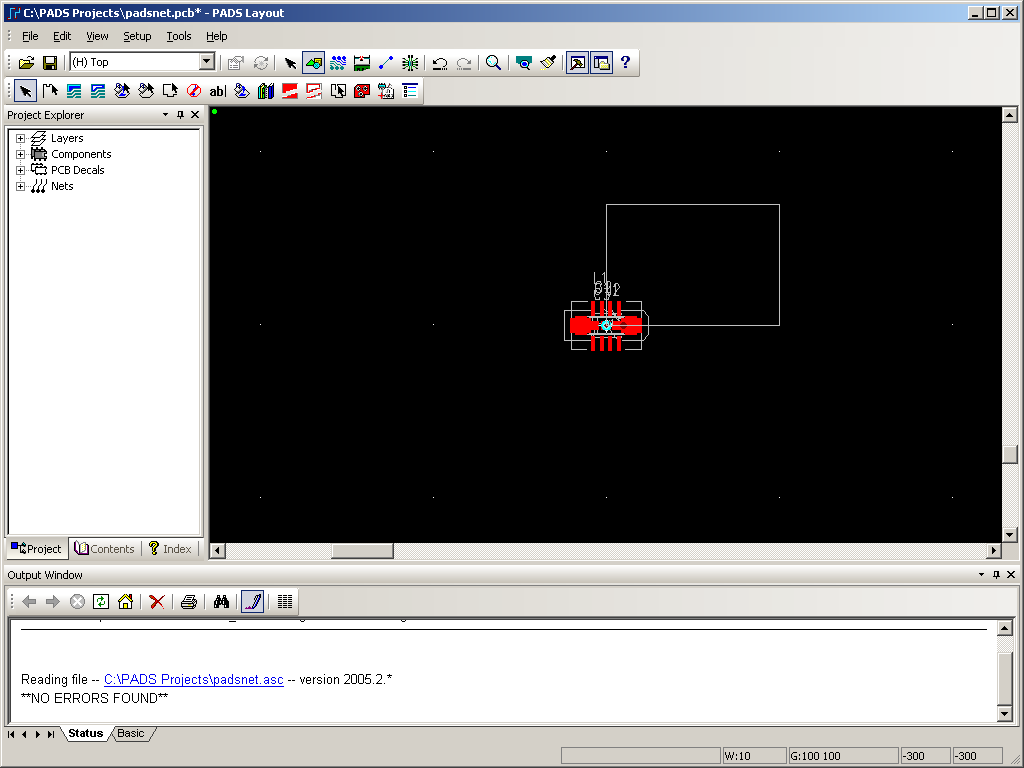
Your PADS Layout window should look similar to the one shown below.
2.4 Setup the Board Layers
Before placing the components on the board, you should modify the
board's Layer Definitions. Select
Setup > Layer
Definition... to open the Layers Setup dialog.
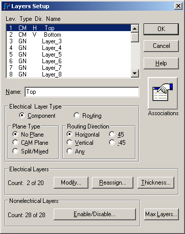
Our board will only need two electrical layers. If more than two
electrical layers are assigned, press the
Modify...
button and enter
2 in the
popup window to fix this.
It is also recommended that you disable any unused layers. Click
on the
Enable/Disable...
button to display the Enable/Disable Layers window.
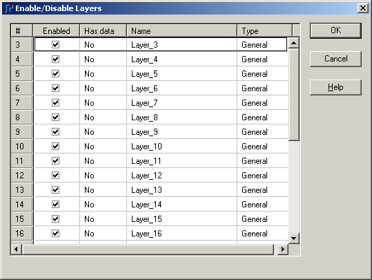
Uncheck layers 3 to 20 and layer 25. Press OK to return to the
Layer Setup window and then press OK again to confirm your changes.
2.5 Positioning circuit components
To make it easier to select individual parts, select
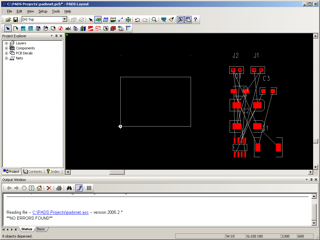
Tools > Disperse
Components. This will reposition the components around the
perimeter of the board, as shown below.
With nothing selected, right-click in an empty area and select the
Select Components option from the context menu.
You can now begin placing the components within the board outline using
drag and drop.
To rotate components, press Ctrl + R.
To flip a component to the opposite side of the board, press Ctrl + F.
One possible layout is shown below.
Note: You may need to resize the placement grid to fit all of the parts
on the board. Use the modeless grid command, G, to resize the
grid. Ex: type
g 50 to set
the grid interval to 50 mils.
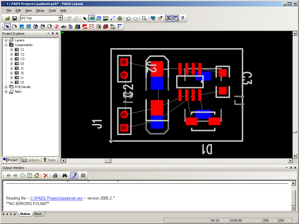
2.6 Position the Reference Designators
You should now take the time to reposition the reference designators
for your design. With nothing selected, right-click and choose
Select Documentation
from the context menu. You can now click and drag the reference
designators to reposition them as shown below.
2.7 Save your PCB Layout.
Select
File
> Save and save the file as
H:\PADS
Tutorial\Tutorial.pcb.
Close PADS Layout and restore the PADS Logic window. Close the
PADS Layout Link window if it is still open.
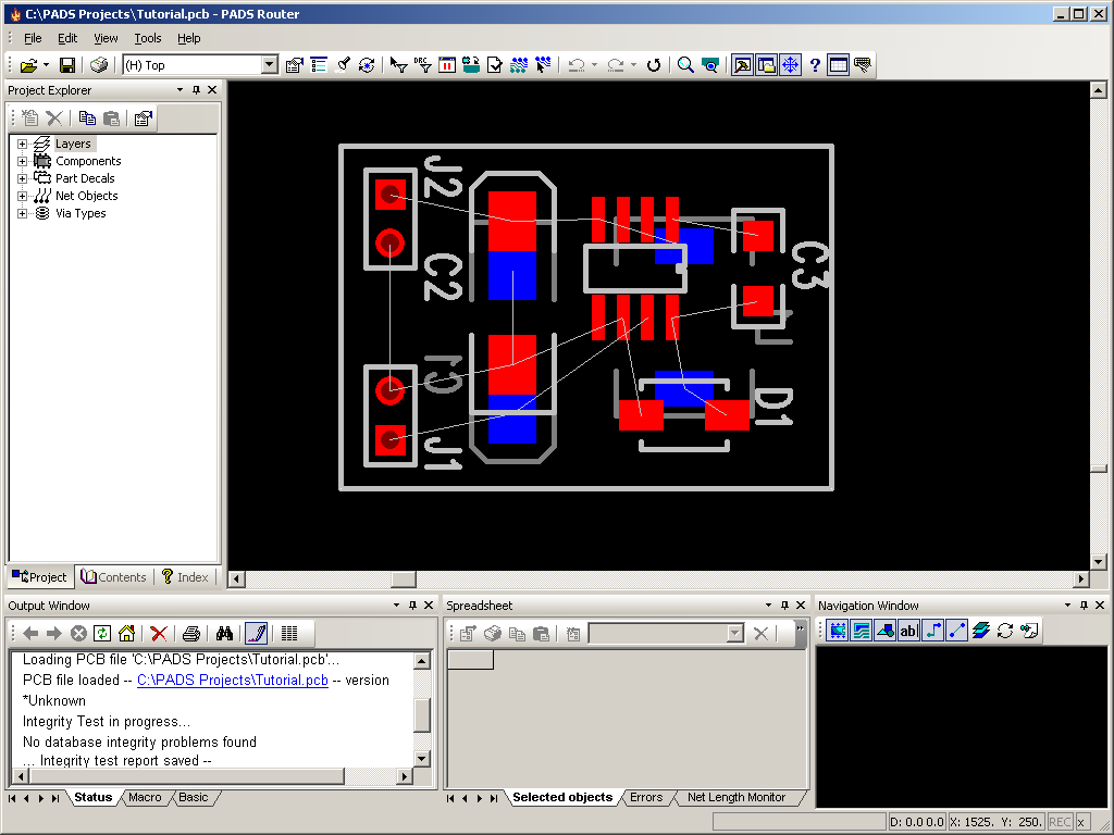
3.1 Linking PADS Logic to PADS Router
You will now connect PADS Logic to PADS Router in the same way that you
connected to PADS Layout. Select
Tools > PADS
Router. The Connect to PADS Router window will appear.
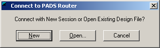
Since we already have a PCB file, select
Open...
Then browse to
H:\PADS
Tutorial and open
Tutorial.pcb.
The PADS Router program should open as shown below.
3.2 View/Modify the Design Properties
To view the current design properties, right-click and select
Properties from the context menu. This will open the Design
Properties window shown below.
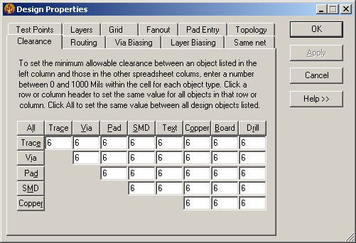
From this window you can adjust a plethora of attributes that affect
your design. Select the various tabs to get an idea of all the
options available. Now select the Routing tab.
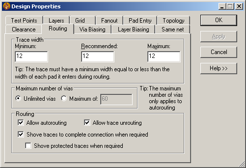
From this tab you can control, among other things, the default width of
your PCB's traces.
Change the Recommended value to 15 and the Maximum value to 20.
Then press OK to confirm your changes.
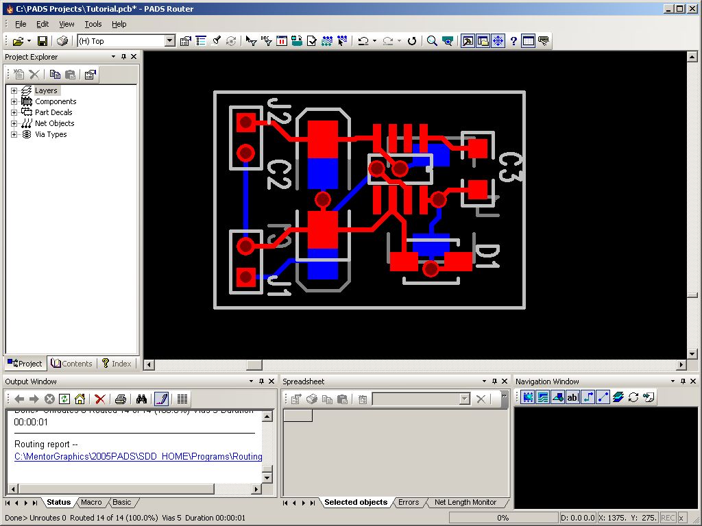
3.3 Use the PADS AutoRouter to route your design.
We will now use the built-in autorouter to route the pcb design.
Select
Tools
> Autoroute > Start to begin the autoroute process.
After a few seconds, the design should be fully routed as shown below.
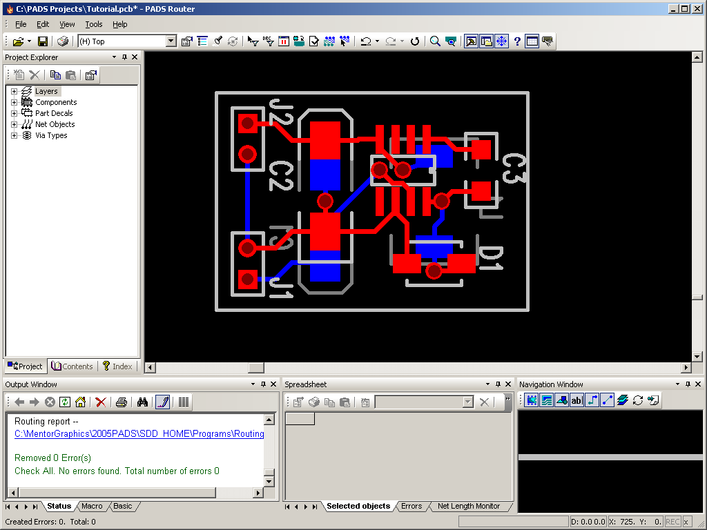
3.4 Verify your design
You should now run a design check to ensure there are no routing errors
with your design. Select
Tools > Verify
Design. The results of the test will appear in the Output
Window located at the bottom right corner of the screen.
3.5 Save your design. Select
File > Save
and then close PADS Router, returning to PADS Logic. Close the
PADS Router Link dialog if it is still open.
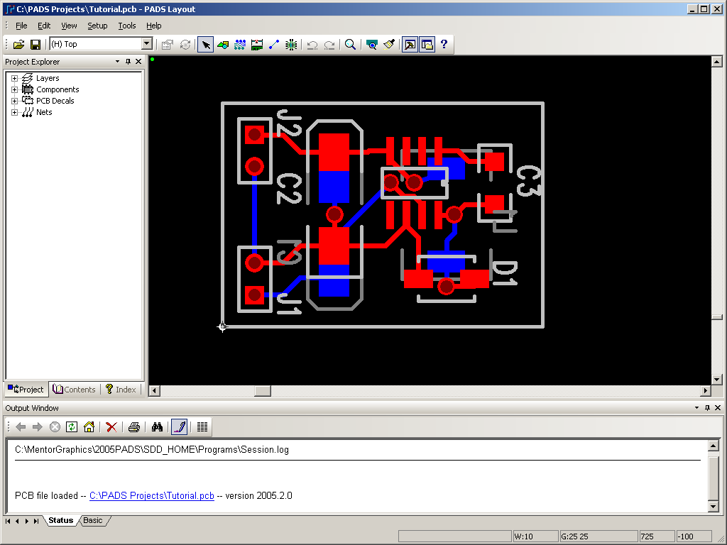
4.1 Linking PADS Logic to
PADS Layout.
You will now connect to PADS Layout again and complete the final steps
in your design. Select Tools > PADS Layout to open the Connect
to PADS Layout window. Select
Open...,
browse to
H:\PADS
Tutorial and open
Tutorial.pcb.
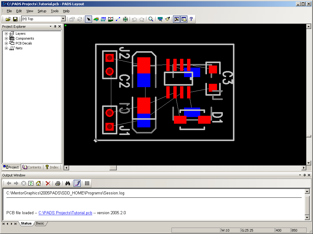
PADS Layout should open, displaying your fully routed design.
4.2 Adding Copper Pours to your PCB
You will now add a copper pour to each side of your PCB. Enable
the drafting toolbar by pressing the
button.
Now press the

button to
enter Copper Pour Mode.
Move the cursor over the origin and click once to start drawing the
outline of the copper pour.
Move the cursor to location 0,700 and click to draw the left edge.
Move the cursor to location 1000,700 and click to draw the top edge.
Move the cursor to location 1000, 0 and double click to complete the
copper pour outline.
The Add Drafting should appear as shown below.
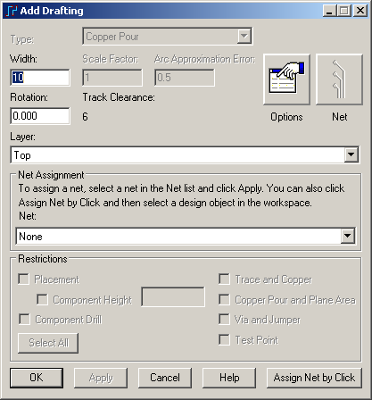
Select Top from the
Layer
dropdown list and select GND from the
Net
dropdown list. Press OK.
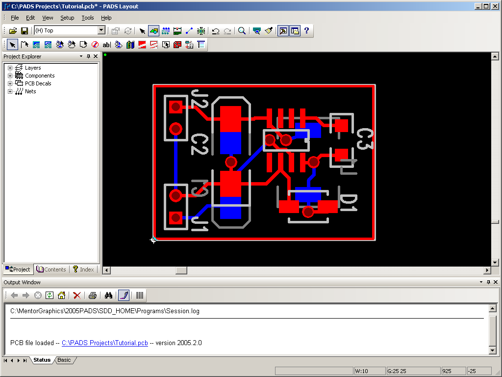
Repeat this process using the same coordinates and choosing Bottom for
the Layer. Select GND for the Net.
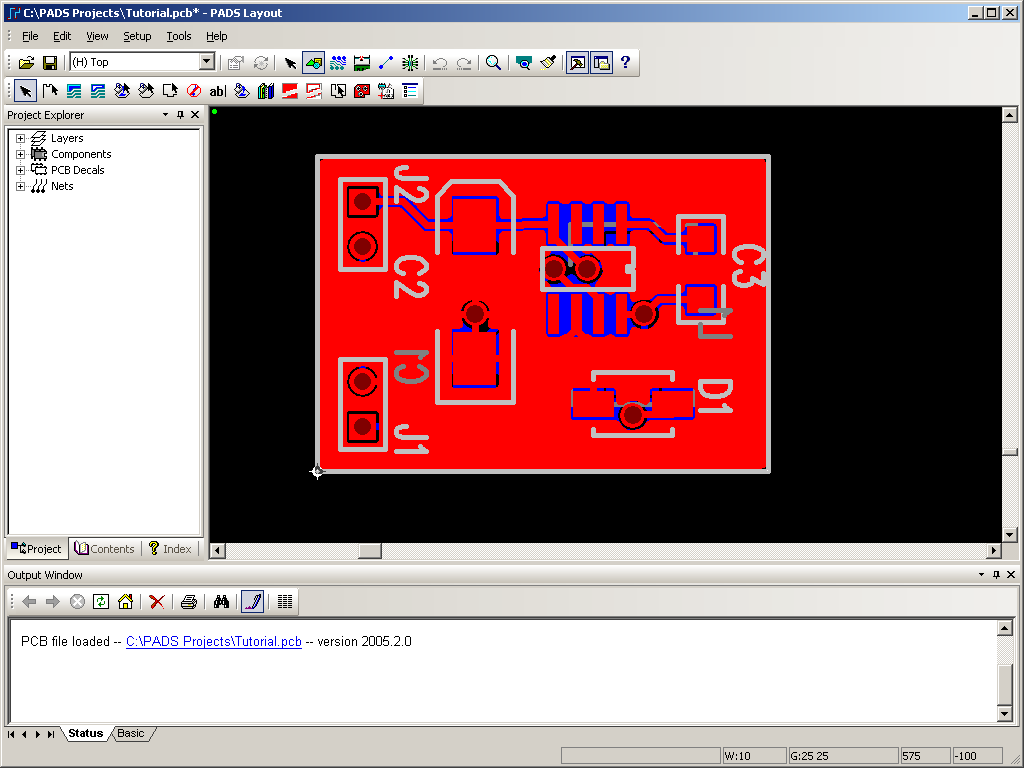
After the copper pours have been added, the design window should appear
as shown below.
Note: If you need to re-route your design, you will need to
remove the
copper pours and save your file before opening it in PADS Router.
If
you fail to do this, PADS Router may not correctly route your PCB.
4.3 Flooding your design.
You will now flood your design, filling in the copper pours with
copper. Select
Tools > Pour
Manager to open the Pour Manager window.
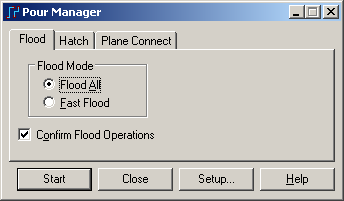
Press
Start
to begin the flood process. If there were no errors, close the
Pour Manager. Your design window should now look similar to the
image below.
If there were any errors, press the
Setup button
to open the Options > Thermals window.
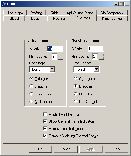
Any copper pour errors can often be corrected by changing the type or
width of the thermal spokes. Changing the type to 'Flood Over'
should always prevent the 'too few spokes generated' error. This,
of course, changes the method used to connect the copper pour to vias
and pads of the same net. Note: Not all copper pour errors are
critical, it may not be deemed necessary to modify the Thermals
parameters.
4.4 Verify Design
You should now check your completed design for errors. Select
Tools > Verify
Design to open the Verify Design window.
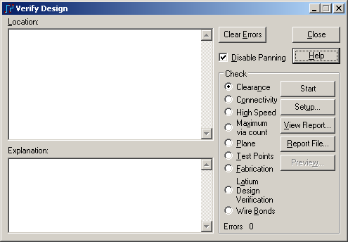
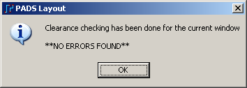
Select Clearance from the Check list and press start. If there
are no errors, the following dialog will be displayed.
Press OK and select Connectivity from the Check list. Press Start
to run the check. If there were no errors, close the Verify
Design window. If any errors were detected, you should locate the
error image on your design and correct the problem.
Note: If you need to re-route your design, you will need to
remove the copper pours and save your file before opening it in PADS
Router. If you fail to do this, PADS Router may not correctly
route your PCB.
4.5 Save your design. Select
File > Save
to save your completed PCB design.
The steps needed to generate the
appropriate gerber files will vary depending on the number of layers
used and the PCB service that will be creating the board. This
section will show the steps needed to create gerber files for a
PCBExpress E2 2-Layer Board.
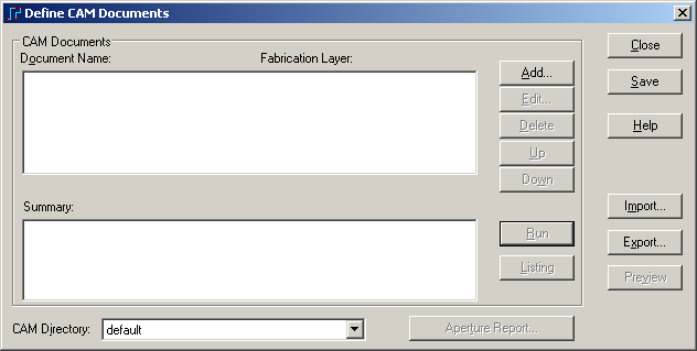
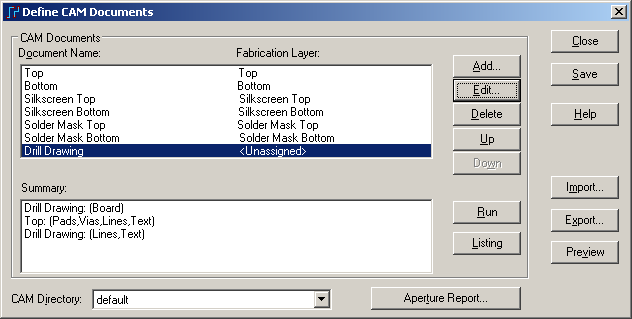
5.1 Select
File > CAM
to open the Define CAM Documents window.
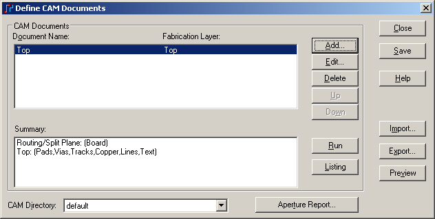
5.2 Top Layer
Press the
Add...
button to display the Add Document window.
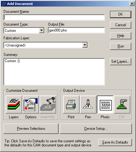
Type
Top
in the Document Name field.
Select
Routing/Split
Plane from the Document Type dropdown list and select
Top from the
popup window.
Press the
Layers
button to open the Select Items window.
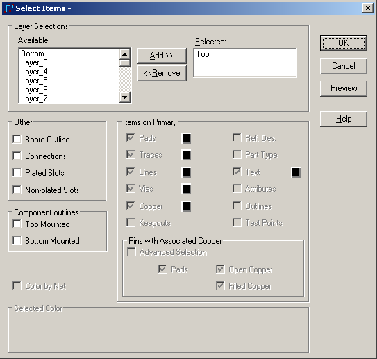
Check the
Board
Outline checkbox and press OK. The Add Document window
should look like the one below.
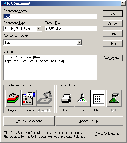
Press the
Device
Setup button to display the Photo Plotter Setup window.
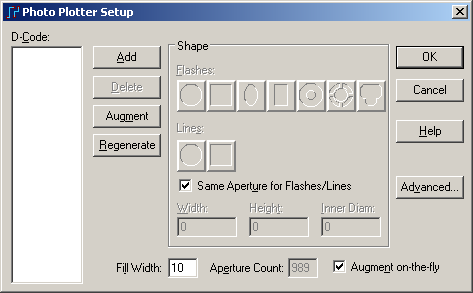
Press the
Regenerate
button and click yes. Press OK.
Press the
Options
button to display the Plot Options window.
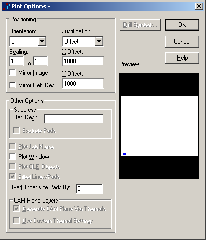
Change the Justification setting to
Scale to Fit
and press OK.
Press the
Preview
Selections button on the Add Document window to verify your
settings.
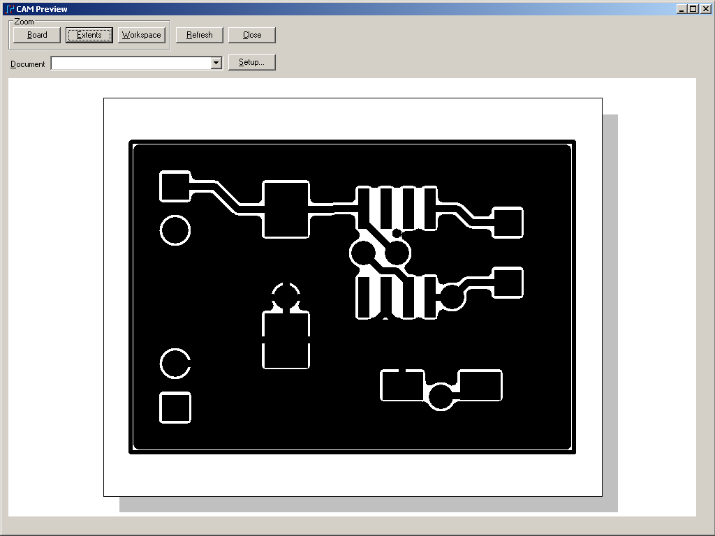
If everything looks correct, close the preview window and then press OK
to add the Top document.
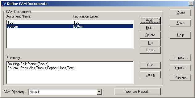
5.3 Bottom Layer
Repeat part 5.2, substituting the
Bottom Layer
for the Top Layer in each step.
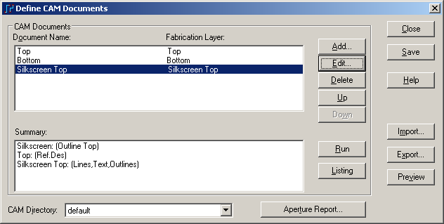
5.4 Silkscreen Top
Press the
Add...
button.
Type
Silkscreen
Top for the Document Name.
Select
Silkscreen from the Document Type list
and then select
Top from the
popup window.
Press the
Layers button to open the Select
Items window. Select
Top from the
Selected List and uncheck
Part Type.
Press OK.
Press the
Options
button and set the Justification to
Scale to Fit.
Press OK.
Press the
Preview
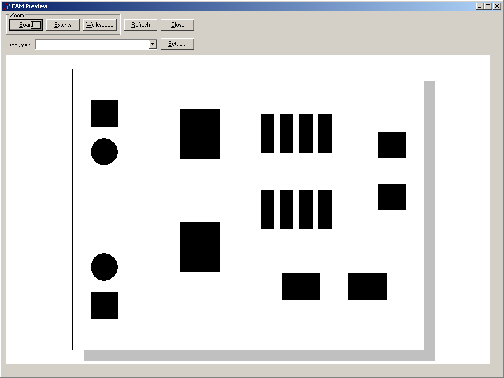
Selections button to verify your design.
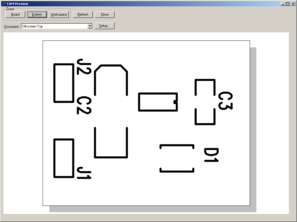
Close the preview and press OK to add the Silkscreen Top document.
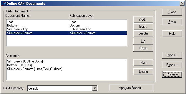
5.5 Silkscreen Bottom
Repeat Section 5.4, substituting Silkscreen Bottom for Silkscreen Top.
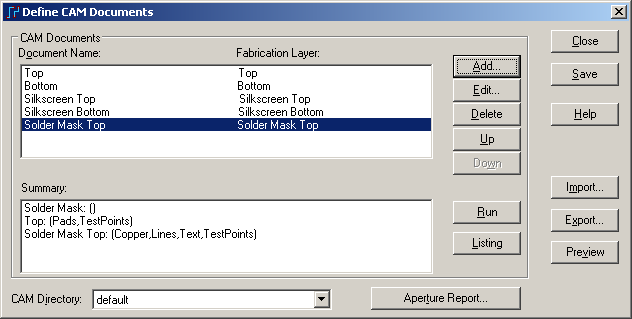
5.6 Solder Mask Top
Press the
Add...
button.
Type
Solder
Mask Top for the Document Name.
Select
Solder
Mask from the Document Type dropdown list and then select
Top from the
popup list.
Press the
Options
button and set the Justification to
Scale to Fit.
Press OK.
Press the
Preview
Selections button to verify your design.
Close the preview and press OK to add the Solder Mask Top document.
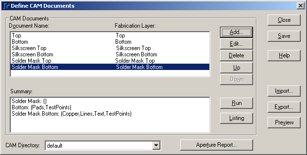
5.7 Solder Mask Bottom.
Repeat Section 5.6, substituting Solder Mask Bottom for Solder Mask Top.
5.8 Drill Drawing
Press the
Add...
button.
Type
Drill
Drawing for the Document Name.
Select
Drill
Drawing from the Document Type dropdown list and then select
Top from the
popup list.
Press the
Options
button and set the Justification to
Scale to Fit.
Press the
Drill
Symbols button and enter
1000 for
Location X.
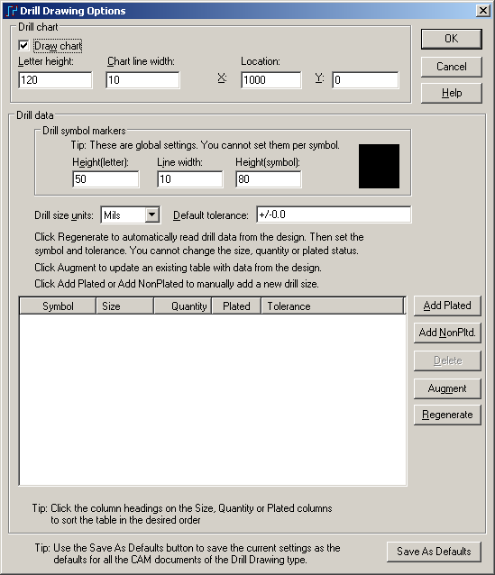
Press OK to close the Drill Drawing Options and Press OK again to
return to the Add Document window.
Press the
Preview
Selections button to verify your design.
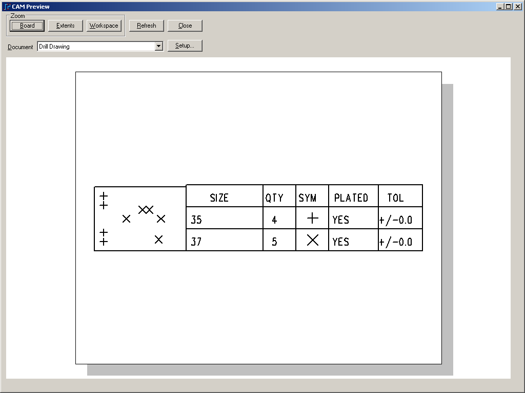
Close the preview and press OK to add the Drill Drawing document.
5.9 NC Drill Document
Press the
Add...
button.
Type
NC Drill
for the Document Name.
Select
NC
Drill from the Document Type dropdown list.
Press the
Preview
Selections button to verify your design.
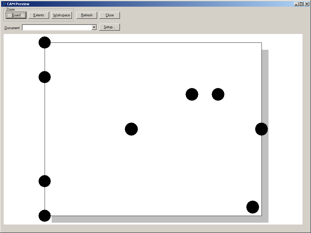
Close the preview and press OK to add the NC Drill document.
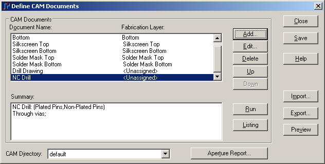
5.10 Generate the Gerber Files
Click on the
CAM
Directory dropdown and select
<Create>.
Enter
H:\PADS
Tutorial\Cam\ for the CAM Subdirectory. Press OK.
Highlight all of the documents and press Run.
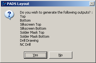
Click Yes to generate the Gerber Files.
After the files have been successfully generated, press Save and then
close the CAM Documents window.
5.11 Verify Gerber Files
Before sending your Gerber Files to the PCB Company, it is recommended
that you verify them with an external tool.
PCBExpress recommends using the PentaLogix ViewMate Gerber Viewer.
http://www.pentalogix.com/Download/download.html
You have now completed the Mentor
Graphics PADS Tutorial.